小米 sells a small little wifi camera which works quite painlessly.
I’ve bought several over the last few years.
My recent ones don’t work oversea’s though (which is where I install them).
Its extremely bogus selling equipment that is limited to a country, especially when they don’t tell you about it.
Annoying, as my older models aren’t “region locked”, but the newer ones are.
There is a fix for it, although it will likely get more difficult to patch at xiaomi’s whim.
If so, I’ll probably stop buying the camera’s. Lovely how vendors want to mess with customers…
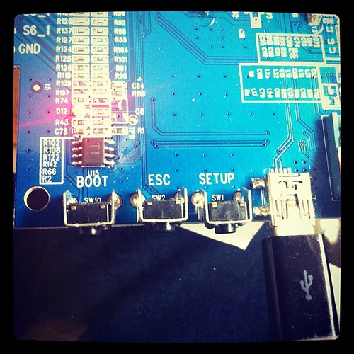
—
First up, enable telnet on the camera.
Get an SD card or take the card out of the camera.
Create a folder named test on the card.
Create a plain text file called equip_test.sh in that folder, and add the following bash script:
#!/bin/sh

# Telnet

if [ ! -f "/etc/init.d/S88telnet" ]; then

echo "#!/bin/sh" > /etc/init.d/S88telnet

echo "telnetd &" >> /etc/init.d/S88telnet

chmod 755 /etc/init.d/S88telnet

fi

dr=`dirname $0`

# fix bootcycle

mv $dr/equip_test.sh $dr/equip_test.sh.moved

reboot
The script will enable telnet on the camera, and then rename the script so it doesn’t run again on the next boot.
Stick the prepared card into the camera, power on, and it should reboot (twice).
If you check the open ports on the camera ip you should now see port 23 (telnet) is open.
Login with the default user/pass (as below) via telnet
User: root

Password: 1234qwer
Once telnet’d in, enter the following, line by line –
Find and kill the watchdog process
killall watch_process
Find and kill /home/cloud process so we can edit it without the watchdog watch_process restarting it
killall cloud
Change the check within /home/cloud executable to query a fake domain so it never returns a failure, then reboot.
 sed -i  's|api.xiaoyi.com/v4/ipc/check_did|api.xiaoyi.foo/v4/ipc/check_did|g' /home/cloud

 reboot
Notes – The camera checks for the country by running an executable called /home/cloud
This calls an api at api.xiaoyi.com which does a ip check, then returns a true or false value if it thinks you’re in China or not. We change the /home/cloud executable ip check call to a bad url, which means it can’t perform its check.
Worked on my camera’s running version 1.8.6.1Q_201607271501
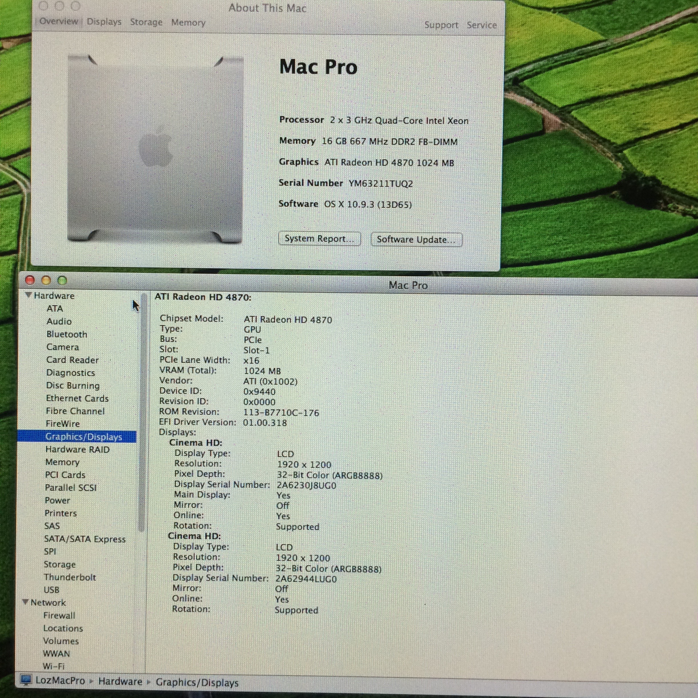
I have a couple of older Mac Pro desktops that I tend to.
As my machines usually get upgraded to the max, they’re still pretty darn useful.
Currently they’re all Dual Quad Core 3Ghz / 16G Ram 1,1->2,1 flashed, which is more than enough for dev purposes.
Sadly though, they still have the original graphics cards – rather crappy 7300GT’s.
One of the issues with the Mac Pro 1,1 is that in Yosemite* the original graphics cards aren’t really supported.
*Sure Yosemite isn’t really supported either, but it does work after a bit of EFI boot mangling.
You can work around things, by having a newer NVidia card (i.e. anything 6XX and above), but then you lose boot graphics till the OS loads drivers.
As I sort of quite need boot graphics due to the bootloader side of things getting borked on occasion, I thought I’d source myself a compatible card.
There aren’t really that many options unfortunately for vintage equipment, its mostly 8800GT’s that are at least 5 years+, and priced at silly money.
There are other options though – certain PC graphics cards are usable.
As a Mac Pro 1,1 (2,1), it needs a card that:
#1 – Shipped on a Mac Pro 1,1 or 2,1 (so that AMD created an _EBC_ based Mac BIOS).
#2 – Has a flashable BIOS. This rules out most of the NVidia’s of that era, so its a select number of ATI cards.
Netkas.org is a good source of reading for that sort of thing.
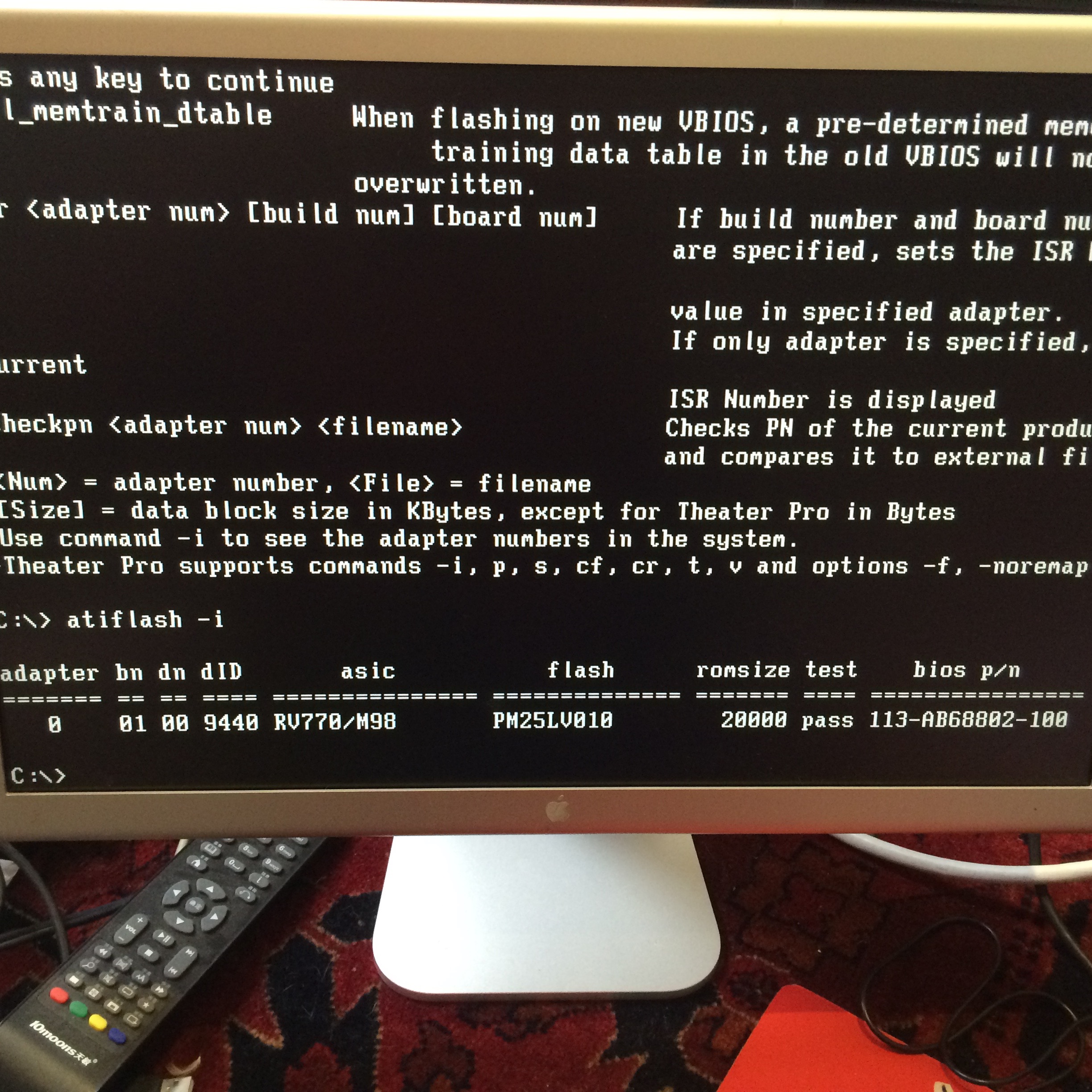
ATI 4870 appears to be flashable, and wasn’t too “$$ bills yo!” on Taobao
So, sourced myself a 4870 1G card (235RMB w/shipping), and set to work.
There is a wealth of information out there about flashing, but unfortunately all the links appear to be pretty dead.
The general consensus is to dump the original firmware, then patch it yourself. There are tools for this, but they don’t really work. Cindori’s Zeus et al..
I tried to do this inside the Mac Pro itself, but it wasn’t having any of it, and didn’t like the perfectly fine DOS USB key(s) I made. Luckily I also had a Windows box available to dump / flash.
Fun and games with PSU connectors later, I booted off a DOS boot disk, used ATIFlash to dump my original rom, then shutdown again.
Stuck the USB key back in my laptop, used a ROM I found inside Zeus (show package contents, copy the 4870EFI.ROM out) + patch that with my dumped rom using fixrom.py from here – http://forum.netkas.org/index.php/topic,692.0.html and the patch instructions here – http://forums.macrumors.com/threads/race-to-dump-the-4870-rom-whos-first.661681/page-14#post-7297669
Copied the patched rom back onto the USB, rebooted off again into the DOS boot disk on my Window box, and flashed the new patched EBC rom bios.
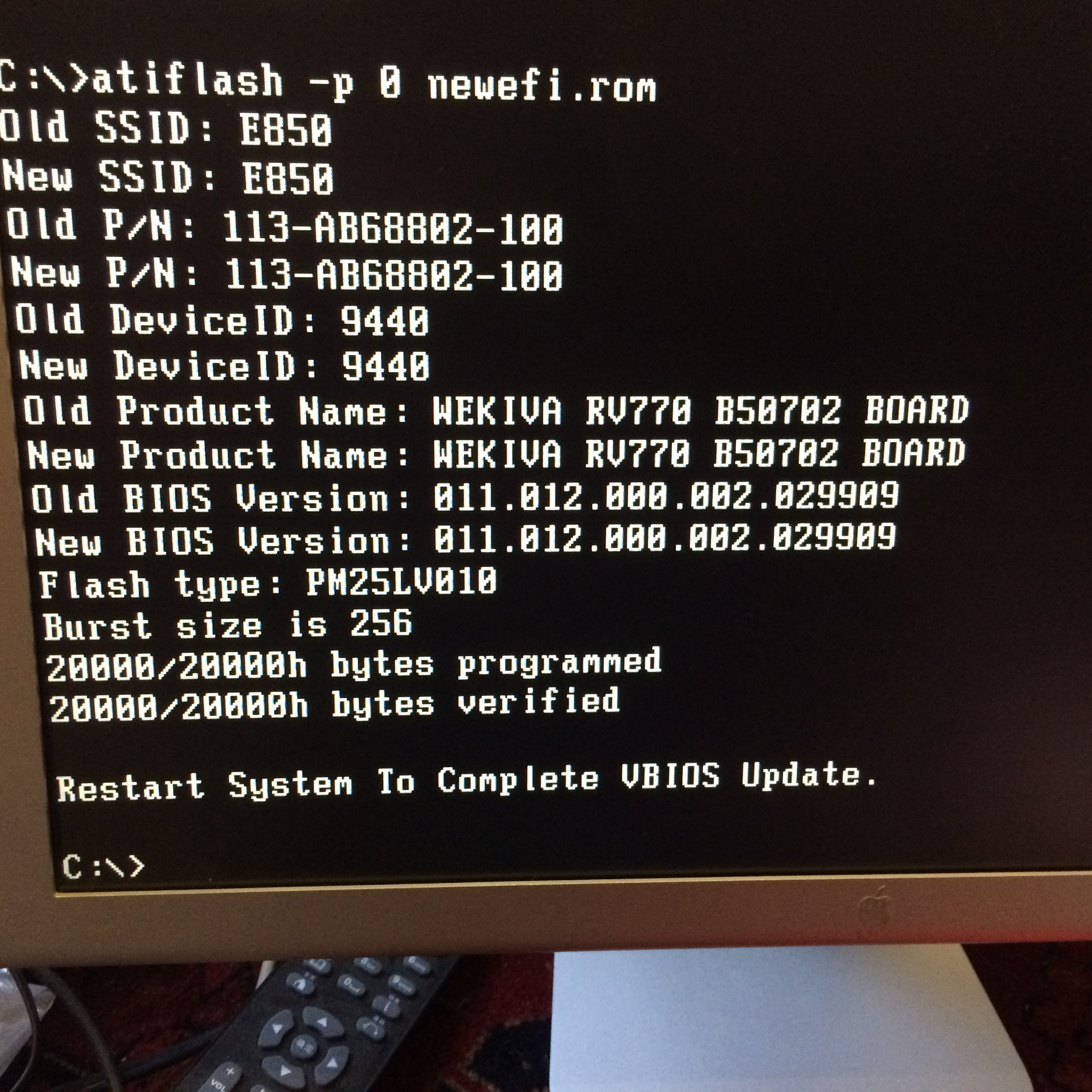
A few minutes of recabling later on the Mac, I got a nice boot screen off the card.
Works fine in OSX too (sleep etc appear to be fine).
As this was a royal pain in the ass, I have the pre-patched rom here – ROM
Its specifically for the 4870 card I have, so don’t randomly flash to your 4870 card, unless the part number matches. My P/N is below.
Radeon HD4870 1G Dual DVI
PN 288-20E85-230AC
Enjoy.
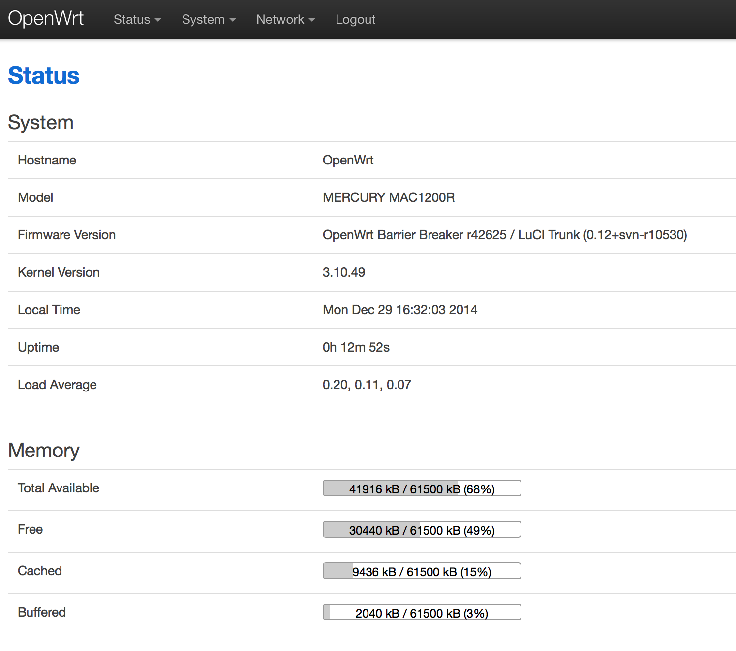
The Mercury MAC1200R (TPLINK WR6300) is one of the cheapest AC based routers on the planet, as I have a few AC devices I thought I’d buy one to try out. They’re available for under RMB120 or so online.
Mercury hardware is TPLink hardware, albeit using a different name. Same stuff, same factory, different casing.
The router has 64M ram, and 8M flash. CPU / Wifi AR9344 / QCA9882
OpenWRT says it has support, so I had a quick go at taking a look at flashing one.
First steps:
Open up the unit (remove the 2 screws underneath, then use a spare credit card or similar to jam open the plastic case).
The serial headers are to the right of the SoC.
You’ll need a rs232 to ttl or usb to ttl adaptor.
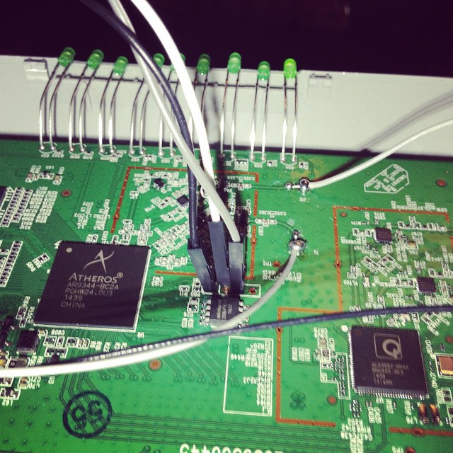
Pin 1 is GND
Pin 2 is TX (connect to rx)
Pin 3 is RX (connect to tx)
Pin 4 is VCC (don’t connect).
Port speeds are 115200,8,n,1
Connect up, and you should see a flurry of activity on boot.
To get into the bootloader (uBoot), you’ll need to type tpl
May take a few tries, so prepare to pull power and retry again, and again till you get in.
You’ll need a TFTPD server running on 192.168.1.100 to push files over. My Mac no haz ethernet (and Thunderbolt to Ethernet is crud), so I use my venerable X40 and tftpd software.
Firmware is up here. (Or you can compile your own) -> http://pan.baidu.com/s/1hqkVOfa
Firmware locations in flash (see below)
printenv

bootargs=console=ttyS0,115200 root=31:02 rootfstype=jffs2 init=/sbin/init mtdparts=ath-nor0:256k(u-boot),64k(u-boot-env),6336k(rootfs),1408k(uImage),64k(mib0),64k(ART)

bootcmd=bootm 0x9f020000

bootdelay=1

baudrate=115200

ethaddr=0xba:0xbe:0xfa:0xce:0x08:0x41

ipaddr=192.168.1.111

serverip=192.168.1.100

dir=

lu=tftp 0x80060000 ${dir}u-boot.bin&&erase 0x9f000000 +$filesize&&cp.b $fileaddr 0x9f000000 $filesize

lf=tftp 0x80060000 ${dir}db12x${bc}-jffs2&&erase 0x9f050000 +0x630000&&cp.b $fileaddr 0x9f050000 $filesize

lk=tftp 0x80060000 ${dir}vmlinux${bc}.lzma.uImage&&erase 0x9f680000 +$filesize&&cp.b $fileaddr 0x9f680000 $filesize

stdin=serial

stdout=serial

stderr=serial

ethact=eth0
Environment size: 686/65532 bytes
Upload to the uBoot
U-Boot 1.1.4--LSDK-10.1.389 (Apr 9 2014 - 15:23:02)
U-Boot DB120
Wasp 1.2
DRAM: 64 MB
Flash Manuf Id 0xef, DeviceId0 0x40, DeviceId1 0x17
flash size 8MB, sector count = 128
Flash: 8 MB
Using default environment
In: serial
Out: serial
Err: serial
Net: ag934x_enet_initialize...
No valid address in Flash. Using fixed address
No valid address in Flash. Using fixed address
wasp reset mask:c02200
WASP ----> S27 PHY
s27 reg init
: cfg1 0x80000000 cfg2 0x7114
eth0: ba:be:fa:ce:08:41
athrs27_phy_setup ATHR_PHY_CONTROL 4 :1000
athrs27_phy_setup ATHR_PHY_SPEC_STAUS 4 :10
eth0 up
WASP ----> S27 PHY
s27 reg init lan
ATHRS27: resetting s27
ATHRS27: s27 reset done
: cfg1 0x800c0000 cfg2 0x7214
eth1: ba:be:fa:ce:08:41
athrs27_phy_setup ATHR_PHY_CONTROL 0 :1000
athrs27_phy_setup ATHR_PHY_SPEC_STAUS 0 :10
athrs27_phy_setup ATHR_PHY_CONTROL 1 :1000
athrs27_phy_setup ATHR_PHY_SPEC_STAUS 1 :10
athrs27_phy_setup ATHR_PHY_CONTROL 2 :1000
athrs27_phy_setup ATHR_PHY_SPEC_STAUS 2 :10
athrs27_phy_setup ATHR_PHY_CONTROL 3 :1000
athrs27_phy_setup ATHR_PHY_SPEC_STAUS 3 :10
eth1 up
eth0, eth1
Setting 0xb8116290 to 0x30602d0f
Autobooting in 1 seconds
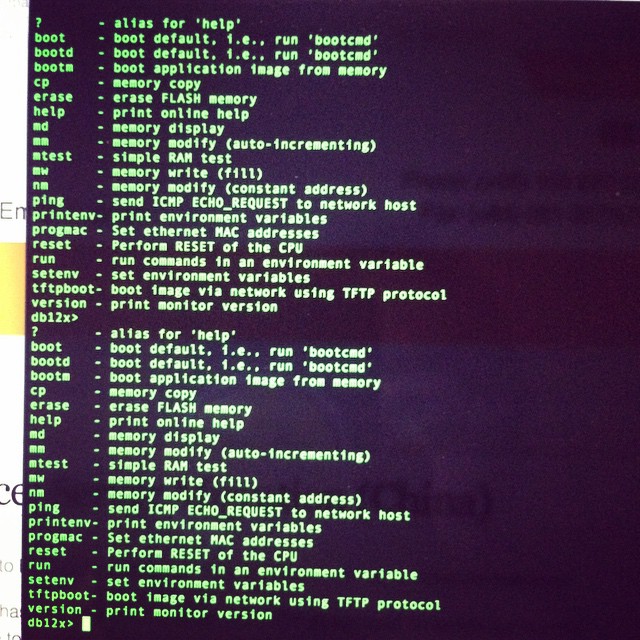
db12x>
db12x> tftpboot 0x81000000 image.bin
eth1 link down
enet0 port4 up
dup 1 speed 100
Using eth0 device
TFTP from server 192.168.1.100; our IP address is 192.168.1.111
Filename 'image.bin'.
Load address: 0x81000000
Loading: #################################################################
#################################################################
#################################################################
#################################################################
#################################################################
#################################################################
#################################################################
#################################################################
#################################################################
##############################
done
Bytes transferred = 3145732 (300004 hex)
db12x> erase 0x9f020000 +0x3c0000
Erasing flash... ............................................................
Erased 60 sectors
db12x> cp.b 0x81000000 0x9f020000 0x3c0000
Copy to Flash... ............................................................done
db12x> bootm 9f020000
It should boot into OpenWRT, you can flash from there.
...[long kernel bootlogs redacted]
- init complete -
BusyBox v1.22.1 (2014-12-15 18:46:26 CST) built-in shell (ash)
Enter 'help' for a list of built-in commands.
_______ ________ __
| |.-----.-----.-----.| | | |.----.| |_
| - || _ | -__| || | | || _|| _|
|_______|| __|_____|__|__||________||__| |____|
|__| W I R E L E S S F R E E D O M
-----------------------------------------------------
BARRIER BREAKER (14.07, r42625)
-----------------------------------------------------
* 1/2 oz Galliano Pour all ingredients into
* 4 oz cold Coffee an irish coffee mug filled
* 1 1/2 oz Dark Rum with crushed ice. Stir.
* 2 tsp. Creme de Cacao
-----------------------------------------------------
cat /proc/mtd
dev: size erasesize name
mtd0: 00020000 00010000 "u-boot"
mtd1: 0010206c 00010000 "kernel"
mtd2: 006cdf94 00010000 "rootfs"
mtd3: 004d0000 00010000 "rootfs_data"
mtd4: 00010000 00010000 "art"
mtd5: 007d0000 00010000 "firmware"
I highly recommend replacing the bootloader with an unlocked one.
i.e. this one – https://github.com/pepe2k/u-boot_mod
Bootloader sits at 0x9f000000 and is 64kb in size.
Suggest load in ram at 0x80060000 like they do, and flash from there.
eg from the bootloader –
tfpboot 0x80060000 uboot.bin

erase 0x9f000000 +0x20000

cp.b 0x80060000 0x9f000000 0x20000
Pray that it didn’t mess up (or you need an spi flasher…), and reboot!
Other bits n bobs –
You’ll need to adjust the opkg.conf file
ssh into the router @ 192.168.1.1 / root / root
mv /etc/opkg.conf /etc/opkg.conf.orig
echo 'dest root /
dest ram /tmp
lists_dir ext /var/opkg-lists
option overlay_root /overlay
src/gz barrier_breaker_base http://downloads.openwrt.org/barrier_breaker/14.07/ar71xx/generic/packages/base
src/gz barrier_breaker_management http://downloads.openwrt.org/barrier_breaker/14.07/ar71xx/generic/packages/management
src/gz barrier_breaker_oldpackages http://downloads.openwrt.org/barrier_breaker/14.07/ar71xx/generic/packages/oldpackages
src/gz barrier_breaker_packages http://downloads.openwrt.org/barrier_breaker/14.07/ar71xx/generic/packages/packages
src/gz barrier_breaker_routing http://downloads.openwrt.org/barrier_breaker/14.07/ar71xx/generic/packages/routing
src/gz barrier_breaker_telephony http://downloads.openwrt.org/barrier_breaker/14.07/ar71xx/generic/packages/telephony
src/gz barrier_breaker_luci http://downloads.openwrt.org/barrier_breaker/14.07/ar71xx/generic/packages/luci
#src/gz barrier_breaker_base http://downloads.openwrt.org/snapshots/trunk/ar71xx/packages/base
#src/gz barrier_breaker_management http://downloads.openwrt.org/snapshots/trunk/ar71xx/packages/management
#src/gz barrier_breaker_oldpackages http://downloads.openwrt.org/snapshots/trunk/ar71xx/packages/oldpackages
#src/gz barrier_breaker_packages http://downloads.openwrt.org/snapshots/trunk/ar71xx/packages/packages
#src/gz barrier_breaker_routing http://downloads.openwrt.org/snapshots/trunk/ar71xx/packages/routing
#src/gz barrier_breaker_telephony http://downloads.openwrt.org/snapshots/trunk/ar71xx/packages/telephony' >> /etc/opkg.conf
…and install Luci (the openwrt webui)
opkg update

opkg install luci
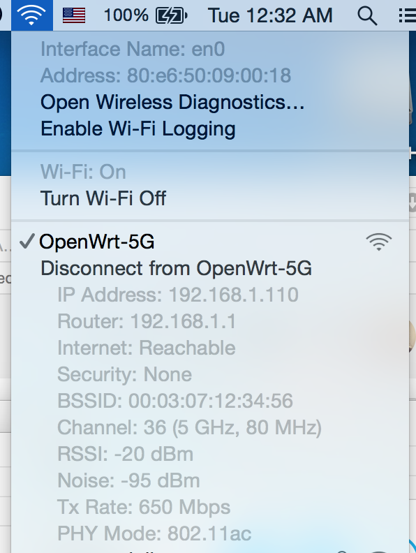
You should be able to visit http://192.168.1.1 and start changing settings.
In January, I upgraded to 100M fibre, and paid upfront for the year (RMB2800).
While I was on vacation, my FTTB at home stopped working, so we called Shanghai Telecom.
What had actually happened was that there was a screwup with the account setup, and they’d put me on a monthly bill *and* 100M.
After 6 months, they decided that I hadn’t paid my bill, and cancelled my 100M fibre account!
Staff eventually sorted it out, and Telecom gave us a 6 month credit.
Even so, I ended up coming back to a crappy E8 wifi + modem setup and my router set to use DHCP.
The Shanghai Telecom unit was setup for a maximum of 16 wifi devices, and uPNP was disabled, sigh.
I prefer to use my own equipment, as I generally don’t gimp it, so I called Telecom to ask for my “new” account details so I could replace it.
Unfortunately the technician had changed the password, and the 10000 hotline didn’t have the new pass, or the LOID.
I called the install technician who’d installed it in my absence, but he wasn’t very helpful, and told me I couldn’t have it. Surprise…
What to do.
I took a look at their modem, and thought it should be fairly easy to try get the details from it.
Did a bit of googling, and found that it had an accessible serial port, so opened up the unit, and connected it up.
After a bit of cable fiddling, got a connection @ 115200 / 8n1
Cable pinout should be –
GND | MISSING PIN | TX | RX | VCC
I’ll add some photos later.
With some more fiddling around, I got terminal access (accidentally!) with some prudent Ctrl C/ Ctrl Z’ing during the boot process as something crashed and I got a terminal prompt.
Its vxware, although the boot process does look quite linuxy.
Lots of interesting commands..
 > ls -al
telnetd:error:341.568:processInput:440:unrecognized command ls -al
 > help
?
help
logout
exit
quit
reboot
brctl
cat
loglevel
logdest
virtualserver
ddns
df
dumpcfg
dumpmulticfg
dumpmdm
dumpnvram
meminfo
psp
kill
dumpsysinfo
dnsproxy
syslog
echo
ifconfig
ping
ps
pwd
sntp
sysinfo
tftp
voice
wlctl
showOmciStats
omci
omcipm
dumpOmciVoice
dumpOmciEnet
dumpOmciGem
arp
defaultgateway
dhcpserver
dns
lan
lanhosts
passwd
ppp
restoredefault
psiInvalidateCheck
route
save
swversion
uptime
cfgupdate
swupdate
exitOnIdle
wan
btt
oam
laser
overhead
mcpctl
sendInform
wlanpower
zyims_watchdog
atbp
ctrate
testled
ipversionmode
dumptr69soap
lan2lanmcast
telecomaccount
wanlimit
namechange
userinfo
localservice
tcptimewait
atsh
option125Mode
eponlinkper
setponlinkuptime
loidtimewait
phonetest
First up, dump the nvram
> dumpnvram
============NVRAM data============
nvramData.ulVersion=6l
nvramData.szBootline=e=192.168.1.1:ffffff00 h=192.168.1.100 g= r=f f=vmlinux i=bcm963xx_fs_kernel d=1 p=0 c= a=
nvramData.szBoardId=      XPT2542NUR
nvramData.ulMainTpNum=0l
nvramData.ulPsiSize=64l
nvramData.ulNumMacAddrs=10l
nvramData.ucaBaseMacAddr=??Umo
nvramData.pad=
nvramData.ulCheckSumV4=0l
nvramData.gponSerialNumber=
nvramData.gponPassword=
nvramData.cardMode=-1
nvramData.cardNo=  000000000000000000
nvramData.userPasswd=telecomadmin31407623
nvramData.uSerialNumber=32300C4C755116D6F
nvramData.useradminPassword=62pfq
nvramData.wirelessPassword=3yyv3kum
nvramData.wirelessSSID=ChinaNet-WmqQ
nvramData.conntrack_multiple_rate=0
============NVRAM data============
Nice, got the router admin pass already.
– nvramData.userPasswd=telecomadmin31407623
(user is telecomadmin).
I actually needed the login details, this turned out to be via
> dumpmdm
This dumped a rather large xml style file with some interesting bits
[excerpted are some of the good bits – the whole file is huge]
Hmm, telnet, and a password!
Telnet is not enabled by default, nor is FTP.
It also had the pppoe user/pass which was what I was looking for, and the LOID, which I needed to stick into my modem.
Score.
While that was pretty much all I needed, I decided to enable Telnet and FTP to play around.
Ok, so how do we enable telnet?
 > localservice
usage:
   localservice show: show the current telnet/ftp service status.
   localservice telnet enable/disable: set the telnet service enable or disable.
   localservice telnetAccess enable/disable: allow access telnet in wan side or not.
   localservice ftp enable/disable: set the ftp service enable or disable.
   localservice ftpAccess enable/disable: allow access ftp in wan side or not.

 > localservice telnet enable

> localservice show
Current local services status:
Ftp Service: Disable
Ftp Allow Wan Access: No
Telnet Service: Enable
Telnet Allow Wan Access: No

> localservice ftp enable

> localservice show
Current local services status:
Ftp Service: Enable
Ftp Allow Wan Access: No
Telnet Service: Enable
Telnet Allow Wan Access: No
 > save
config saved.
reboot the modem, and see if we can login via ethernet
telnet 192.168.1.1
Trying 192.168.1.1...
Connected to broadcom.home.
Escape character is '^]'.
BCM96838 Broadband Router
Login: telecomadmin
Password:
Login incorrect. Try again.
Login: e8telnet
Password:
 >
Cool, so we now have full access to the device.
There also seems to be a remote monitoring system config’d via devacs.edatahome.com, which maps to a Shanghai Telecom ip.
   http://devacs.edatahome.com:9090/ACS-server/ACS
      http://devacs.edatahome.com:9090/ACS-server/ACS
      hgw
      hgwXXXX1563
and something else called itms.
itms
 itmsXXXX5503
I’ve XXX’d out some of the numbers from my own dump, as I suspect its device / login specific.
I got what I needed though, which was admin access to the modem, despite Shanghai Telecom not telling me.
Would really be nice if they just gave you the PPPoE user/pass and LOID, but that would be too easy…
On my modem, the following were the default passwords:
Console Access (via serial port)
User: admin
Pass: v2mprt
Once in console, you can enable Telnet and FTP.
Telnet (not enabled by default)
User: e8telnet
Pass: e8telnet
FTP (not enabled by default)
User: e8ftp
Pass: e8ftp
To show the http password from console (either local, or via telnet).
dumpnvram
url: http://192.168.1.1
http user: telecomadmin
http pass: (as per nvram, mine was telecomadmin31407623 )
Once in you can see all the important bits. Probably easier to grep the xml file from
dumpmdm
Took me about an hour or so to get to that point, I’m running on my own equipment again, and its not gimped. Worth my time!
Someone from the JammaForums.co.uk emailed me a copy of the firmware in their SD card from a XinYe 138 in 1.
Card looks something like this:

I don’t have one, but I took a quick look at the data provided, and it looks fairly straightforward to “hack”.
It actually took me less than 30 minutes to have most of the good bits extracted from receiving the file!
There are 2 files on the SD card.
One is a 64 byte file called sn.bin which contains this data:

This looks suspiciously like a header, but I haven’t taken a clear look.
The second file is called x3rodl.bin, and contains a Linux firmware in ARM format.
The first few hundred bytes look like this:

Its obviously in ARM format, as the first set of bytes are ARM no-op codes.
00 00 A0 E1, which repeats 8 times.
02 00 00 EA, then…
18 28 6F 01 – Which is a magic word indicating that this contains a zImage (compressed Linux kernel)
18 28 6F 01 = 0x016f2818
Linux code looks something like this for identifying if its a kernel:
if (*(ulong *)(to + 9*4) != LINUX_ZIMAGE_MAGIC) {

        printk("Warning: this binary is not compressed linux kernel image/n");

        printk("zImage magic = 0x%08lx/n", *(ulong *)(to + 9*4));

    } else {

        printk("zImage magic = 0x%08lx/n", *(ulong *)(to + 9*4));

    }
9 * 4 = 36, which is our location, and this happens to have our magic number.
So, we know its a kernel. Its also probably the VIVI bootloader from Samsung, as that uses that style MAGIC.
The following bits of data, contain the setup for the kernel, and the boot code.
This continues on until the compressed kernel+ramdisk. That starts with 1F 8B 08 (gzip header bytes) over at 0x3EF2, until roughly the end of the file.
I extracted that part and had a quick look.
Its about 7.7M size unpacked.
Linux version is: 2.6.36-FriendlyARM
Boot params are:
console=ttySAC0,115200 root=/dev/ram init=/linuxrc initrd=0x51000000,6M ramdisk_size=6144
RAMDISK File System starts at 0x20000, and looks like this:
lawrence$ ls -al

total 24

drwxr-xr-x  13 lawrence  staff   442 Jun 17 23:09 .

drwxr-xr-x   4 lawrence  staff   136 Jun 17 23:08 ..

drwxr-xr-x  51 lawrence  staff  1734 Jun 17 23:09 bin

drwxr-xr-x   2 lawrence  staff    68 Jun 17 23:09 dev

drwxr-xr-x  11 lawrence  staff   374 Jun 17 23:09 etc

-rwxr-xr-x   1 lawrence  staff  3821 Jun 17 23:09 init

-rw-r--r--   1 lawrence  staff  3821 Jun 17 23:09 init~

lrwxrwxrwx   1 lawrence  staff    11 Jun 17 23:09 linuxrc -> bin/busybox

drwxr-xr-x   2 lawrence  staff    68 Jun 17 23:09 proc

drwxr-xr-x   2 lawrence  staff    68 Jun 17 23:09 r

drwxr-xr-x  19 lawrence  staff   646 Jun 17 23:09 sbin

drwxr-xr-x   2 lawrence  staff    68 Jun 17 23:09 sdcard

drwxr-xr-x   4 lawrence  staff   136 Jun 17 23:09 usr
The bootup script for this looks like this:
#! /bin/sh
PATH=/sbin:/bin:/usr/sbin:/usr/bin
runlevel=S
prevlevel=N
umask 022
export PATH runlevel prevlevel
echo st.
#
# Trap CTRL-C &c only in this shell so we can interrupt subprocesses.
#
trap ":" INT QUIT TSTP
/bin/hostname FriendlyARM
/bin/mount -n -t proc proc /proc
cmdline=`cat /proc/cmdline`
ROOT=none
ROOTFLAGS=
ROOTFSTYPE=
NFSROOT=
IP=
INIT=/sbin/init
#run_fs_image=/images/linux/rootfs_xin1arm_sdhotplug.ext3
for x in $cmdline ; do
case $x in
root=*)
ROOT=${x#root=}
;;
rootfstype=*)
ROOTFSTYPE="-t ${x#rootfstype=}"
;;
rootflags=*)
ROOTFLAGS="-o ${x#rootflags=}"
;;
init=*)
INIT=${x#init=}
;;
nfsroot=*)
NFSROOT=${x#nfsroot=}
;;
ip=*)
IP=${x#ip=}
;;
esac
done
if [ ! -z $NFSROOT ] ; then
echo $NFSROOT | sed s/:/\ /g > /dev/x ; read sip dir < /dev/x
echo $IP | sed s/:/\ /g > /dev/x; read cip sip2 gip netmask hostname device autoconf < /dev/x
rm /dev/x
#echo $sip $dir $cip $sip2 $gip $netmask $hostname $device $autoconf
mount -t nfs $NFSROOT /r -o nolock,proto=tcp
#[ -e /r/dev/console ] || exec /bin/sh
elif [ ! -z $run_fs_image ] ; then
#lilxc
#echo $run_fs_image
echo sdroot.
if [ ! -e /dev/mmcblk0p2 ] ; then
echo "p2 not found."
reboot
sleep 5
fi
ROOTFSTYPE="-t ext3"
for i in 1 2 3 4 5 ; do
#/bin/mount -n -o sync -o noatime -o nodiratime -o ro -t vfat /dev/mmcblk0p1 /sdcard && break
/bin/mount -n -o sync -o noatime -o nodiratime -o ro -t ext3 /dev/mmcblk0p2 /sdcard && break
echo Waiting for SD Card...
if [ $i = 4 ] ; then
echo " p2 failed. "
reboot
sleep 5
break;
fi
sleep 1
done
#echo ------begin----------------------------------------
#sleep 1
#lilxc
#ls -l /dev
#sleep 1
#echo -----------------------------------------------
#ls -l /sdcard
#sleep 1
#echo ------end------------------------------------------
#/sbin/losetup /dev/loop0 /sdcard/$run_fs_image
#/bin/mount $ROOTFSTYPE /dev/loop0 /r
#/bin/mount $ROOTFSTYPE -o noatime -o nodiratime -o ro /dev/mmcblk0p2 /r > /dev/null 2>&1
/bin/mount $ROOTFSTYPE -n -o noatime -o nodiratime -o ro /dev/mmcblk0p3 /r > /dev/null 2>&1
mount -o move /sdcard /r/sdcard
#/sbin/losetup /dev/loop1 /r/sdcard/swap
#/sbin/swapon /dev/loop1
else
# /bin/mount -n $ROOTFLAGS $ROOTFSTYPE $ROOT /r
# echo "Readonly mount...(lilxc)"
# mount -n -t yaffs2 -o noatime -o nodiratime -o ro /dev/mtdblock2 /r
# mount -n -t yaffs2 -o noatime -o nodiratime /dev/mtdblock2 /r
mount -n -t yaffs2 -o noatime -o nodiratime -o ro /dev/mtdblock2 /r
if [ -e /r/home/plg/reboot ]; then
umount /r
mount -n -t yaffs2 -o noatime -o nodiratime /dev/mtdblock2 /r
fi
fi
ONE_WIRE_PROC=/proc/driver/one-wire-info
ETC_BASE=/r/etc
[ -d /r/system/etc ] && ETC_BASE=/r/system/etc
[ -e $ETC_BASE/ts.detected ] && . $ETC_BASE/ts.detected
[ -z $CHECK_1WIRE ] && CHECK_1WIRE=Y
if [ $CHECK_1WIRE = "Y" -a -e $ONE_WIRE_PROC ] ; then
if read lcd_type fw_ver tail < $ONE_WIRE_PROC ; then
if [ x$lcd_type = "x0" -a x$fw_ver = "x0" ] ; then
TS_DEV=/dev/touchscreen
else
TS_DEV=/dev/touchscreen-1wire
echo "1Wire touchscreen OK"
fi
if [ -e $ETC_BASE/friendlyarm-ts-input.conf ]; then
sed "s:^\(TSLIB_TSDEVICE=\).*:\1$TS_DEV:g" $ETC_BASE/friendlyarm-ts-input.conf > $ETC_BASE/ts-autodetect.conf
mv $ETC_BASE/ts-autodetect.conf $ETC_BASE/friendlyarm-ts-input.conf -f
echo "CHECK_1WIRE=N" > $ETC_BASE/ts.detected
fi
fi
fi
[ -e /r/etc/friendlyarm-ts-input.conf ] && . /r/etc/friendlyarm-ts-input.conf
[ -e /r/system/etc/friendlyarm-ts-input.conf ] && . /r/system/etc/friendlyarm-ts-input.conf
export TSLIB_TSDEVICE
#lilxc debug here
#/bin/mount -n -o sync -o noatime -o nodiratime -t vfat /dev/mmcblk0p1 /sdcard
#cp /sdcard/lktcmd /r/tmp
#exec /bin/sh
# for running game
umount /proc
exec switch_root /r $INIT /r/dev/console 2>&1
The secondary loader in init looks like this:
#! /bin/sh
PATH=/sbin:/bin:/usr/sbin:/usr/bin:/usr/local/bin:
runlevel=S
prevlevel=N
umask 022
export PATH runlevel prevlevel
#
# Trap CTRL-C &c only in this shell so we can interrupt subprocesses.
#
trap ":" INT QUIT TSTP
/bin/hostname FriendlyARM
[ -e /proc/1 ] || /bin/mount -n -t proc none /proc
[ -e /sys/class ] || /bin/mount -n -t sysfs none /sys
[ -e /dev/tty ] || /bin/mount -t ramfs none /dev
/bin/mount -n -t usbfs none /proc/bus/usb
echo /sbin/mdev > /proc/sys/kernel/hotplug
/sbin/mdev -s
/bin/hotplug
# mounting file system specified in /etc/fstab
mkdir -p /dev/pts
mkdir -p /dev/shm
/bin/mount -n -t devpts none /dev/pts -o mode=0622
/bin/mount -n -t tmpfs tmpfs /dev/shm
/bin/mount -n -t ramfs none /tmp
/bin/mount -n -t ramfs none /var
mkdir -p /var/empty
mkdir -p /var/log
mkdir -p /var/lock
mkdir -p /var/run
mkdir -p /var/tmp
/sbin/hwclock -s
echo " " > /dev/tty1
echo "System starting... " > /dev/tty1
syslogd
#/etc/rc.d/init.d/netd start
#echo " " > /dev/tty1
#echo "Starting networking..." > /dev/tty1
#sleep 1
#/etc/rc.d/init.d/httpd start
#echo " " > /dev/tty1
#echo "Starting web server..." > /dev/tty1
#sleep 1
#/etc/rc.d/init.d/leds start
#echo " " > /dev/tty1
#echo "Starting leds service..." > /dev/tty1
#echo " "
#sleep 1
/etc/rc.d/init.d/mkjoy
#echo " " > /dev/tty1
#echo "System Starting... " > /dev/tty1
#echo " " > /dev/tty1
#echo " " > /dev/tty1
/etc/rc.d/init.d/alsaconf start
#echo "Loading sound card config..." > /dev/tty1
#echo " "
#/sbin/ifconfig lo 127.0.0.1
#/etc/init.d/ifconfig-eth0
#/bin/qtopia &
#echo " " > /dev/tty1
#echo "Starting Qtopia, please waiting..." > /dev/tty1
cd /sdcard
./run.sh
reboot
Fairly easy to reverse!
Refs:
http://www.jammaplus.co.uk/
http://blog.csdn.net/liangkaiming/article/details/6259189
Following up from my previous posts on this, looks like my idea’s are correct about the size of the NAND for setup, and my NAND read stuff works. Yay for me.
Lets recap:
JZ4755 boot sequence is as follows:
CPU powers up.
Checks BOOT_SEL line, takes appropriate action.
boot_sel[1:0]

00	Unused

01	Initialization via USB port: Receives a block of data through the USB (device) port,

and stores it in internal SRAM.

10	Initialization via NAND memory with 512-byte pages at Chip Select 1 (CS1):

11	Initialization via NAND memory with 2048-byte pages at Chip Select 1 (CS1):
In our board, if we press BOOT, this pulls the pin low, so CPU see’s 01, and waits for an IPL from USB.
If we leave it to boot normally, then it reads from NAND.
So far so good.
Lets see if anyone was watching carefully 🙂
Our board NAND chip has a page size of 8192+OOB
Our *CPU Hardware* supports either 512bytes or 2048bytes page size on boot.
Our IPL (aka NAND.BIN) must be 8K in size or less, as the CPU has 8k only, and it copies the bootloader to that obeying BOOT_SEL.
Lets look at what happens.
If I read out the NAND (NREAD 0 8192 0 0) with our carefully set sizing, I see the following:
0000 - 2047 (2k in size) -  DATA  FF 55 55 .. 02 00 0C

2048 - 2549 (512bytes in size)  - BLANK

2560 - 4607 (2k in size) - DATA (padded at end with FF's to 2k size) 21 20 00 .. 85 8c 90+ FF -> 2048 end

4608 - 6655 (2k in size) - DATA  (padded at end with FF's to 2k size)
So, we have roughly about 6k odd of data, out of our 8k max. Its a bit weirdly laid out though, and has some holes in there, so its _not_ correct 🙁
Lets look at the RAW NAND DUMP (NREAD_RAW 0 8192 0 0). Our raw page size is 8192.
Page 0

00000 - 02047 (2k in size) - DATA  FF 55 55 .. 02 00 0C (same as before)

02048 - 02102 (55 bytes)   - (presumed OOB / ECC stuff...) NEW

Page 1

08192 - 10239 (2k in size) - DATA 21 20 00 .. 10 80 00.  Our 85 8c 90 above is actually part of the 55byte sequence, so definitely our NREAD is incorrect, as we're suddenly short data.

10240 - 10294 (55 bytes )  - (presumed OOB / ECC stuff...) NEW

Page 2

16384 - 18431 (2k in size) - DATA (padded with 0's from 17892 - 18431), so our NAND loader data is roughly 5.5KBish.

18432 - 18486 (55 bytes )  - (presumed OOB / ECC stuff...) NEW

Page 3

25026 onwards FF's - so uninitialized.
So, with that, we know that NREAD doesn’t quite work for our first 4 pages (page 0 – 3), and we either need to NREAD_RAW, or possibly use a 2048byte page size in order to read the NAND.BIN properly.
Thats only necessary for the first 4 pages in the NAND though.
Once the NAND.BIN MINIOS bootstrap is running, it should be able to cope with our proper data size.
How does it do that though?
MINIOS Bootloader starts up, as it gets added to the CPU boot sequence detailed above, then it looks for 3 things in 3 places 🙂
Our mystery locations for that are:
Page 61
Page 62
Page 63
Page 61 contains our NAND size stuff, which as we know from above, our Bootloader *can’t* use, as its only 2k or 512byte set at the hardware level initially.
Page 61 in mine has 12 bytes. This looks exceedingly good as I know that my work is, er, working 🙂
USBBoot :> nreadraw 61 24 0 0

Reading RAW from No.0 device No.0 flash....

0x00000000 :00 20 00 00 c0 01 00 00 00 01 00 00
00 20 00 00 = 8192 PAGE SIZE
c0 01 00 00 = 448 OOBSIZE
00 01 00 00 = 256 PAGE PER BLOCK
Lets look at the 3 bytes.
First 16bit word is = 8192 – thats our Page Size
Second 16bit word is = 448 – thats our OOB size (oob = out of block, usually used for CRC or Error etc, as NAND can go BAD if you write to it frequently)
Third 16bit word is = 256 – thats how many pages per block we have.
Block 61, and Block 62 are the same. Basically 62 is a backup of 61. If the NAND.BIN MINIOS loader can’t read Block 61 12 bytes, it tries Block 62. If neither work, you’ll need to reflash, or replace the NAND…
Block 63 contains a whole 10 bytes. This is the UID of the device. Mine is set to 0. Lazy buggers 🙂
Ok, so now we booted, and the MINIOS bootstraploader / NAND.BIN has read our NAND size, then what?
Well, you’ll need to disassemble the code to see (eg as part of my previous post), but essentially it calls the next thing in line.
This can be Linux, or something else. In the board, the OS used is MINIOS, so it loads something else – aka MINIOS.
MINIOS is actually uCOS-II – You can find details on that from Micrium, as they licence it out.
Ingenic has a custom version of uCOS-II for their board. uCOS-II is also a RTOS (Real Time OS).
You can read more on MINIOS here – http://en.wikipedia.org/wiki/MicroC/OS-II
Anyway, lets get back to work, and less chatter 🙂
NAND.BIN passes control onto whatever is sitting at Page 128 (this can be changed, but in the JAMMA board, and in the GameBox GBX-0001), the next loader is at Page 128.
As I don’t have much info on the MINIOS side, I got a lot of this info from other places. Mostly the MINIOS_CFG.INI in the Ingenic FTP Site, plus some gracious help from Joseba Epalza (thanks!) at www.zonadepruebas.com. He supplied a Gamebox dump, and asked me a few questions, which made me re-examine things, which was extremely useful as then I could bounce idea’s and findings off of someone else.
The Gamebox hardware and the Jamma hardware is extremely similar, so the NAND dump in both is good for both of us to double check each others work. Unfortunately, I don’t speak Portuguese Spanish, so we both relied on Google Translate to talk via email today, but we seem to be doing ok 🙂
Onto the tech side again, our secondary loader is, in MINIOS terms, called LOADER.BIN
This sits at Page 128
LOADER.BIN tries to read a file called DEF_BOOT.BIN for configuration settings, as that tells LOADER.BIN where the rest of the filesystem is!
In theory, Page 256 contains
DEF_BOOT.BIN
I need to go back and recheck that now, as my dumps are a bit messy, and I need to check on actual hardware, vs the many whoops I renamed that wrong files I now have messing up my desktop.
I also need to check if I need to read as 2k block size/or raw to get the correct data in these pages, as one place online says that the secondary bootloader (LOADER.BIN) also assumes 2k size.
Other bits:
IMG_BOOT.BIN – bootup code if used.
MINIOS.BIN – the OS.
RES.BIN – Resources used by MINIOS.BIN
The rest… (FAT16 Filesystem which is readable over USB via normal boot)
—
Ignoring my first 8k not quite correct dumped dumps + possibly borked secondary loader stuff, the rest of the data dump looks accurate.
I have what looks like RES.BIN stuff, I have a MINIOS, and I can see interesting things.
Interesting things below:
Dump pos 0x100200 - seems to have the RES.BIN filesystem in mine -
mobile_tv.bin
desktop.bin
udc_battery.bin
sysconfig.bin
toolsbox.bin
calendar.bin
ebook.bin
worldclock.bin
russblock.bin
fmradio.bin
recorder.bin
mp3_compress.bin
viewer.bin
jpgdec.bin
pngdec.bin
bmpdec.bin
gifdec.bin
AudioTag.bin <-- significant, means case sensitive
vplayer.bin
fplayer.bin
aplayer.bin
video.bin
alarm.bin
gameplay.bin
gba_lib.bin
nes_lib.bin
snes_lib.bin
md_lib.bin
ticru_lib.bin
dcDecoder.bin
dvEncoder.bin
dcdv.bin
mpcodecs_ad_liba52.bin
mpcodecs_ad_hwac3.bin
ffmpeg64.bin
ffmpeg_vd_mpegmisc.bin
ffmpeg_vd_mpegmisc2.bin
ffpmeg_vd_mpegvideo.bin
mpcodecs_vs_libmpeg2.bin
ffmpeg_vd_svq3.bin
mpcodecs_vd_realvid.bin
aux_task.bin
desktoplib_simplen.bin
desktoplib_drawer.bin
desktoplib_slide.bin
desktoplib_tradition.bin <- chinese traditional
desktoplib_arena.bin
desktoplib_diorama.bin
So, I know that that part is correct at least, as it really truly looks like proper data 🙂
Other things of note.
Our FAT part of the NAND, that is USB accessible is referred to internally as nfl: (Nand FLash I expect).
Looks like our loader looks for these files in the user side:
nfl:\system\music.img
nfl:\system\ebook.img
nfl:\system\desktop.img
nfl:\system\record.img
nfl:\system\system.cfg
nfl:\system\UPDATE.BIN
Filename strings are NULL terminated.
There is also this:
nfl:\GAME \gamegameList
This seems to be our mapping of game.zip -> proper name file (having taken a look at that).
Which, is why when I added FBANext compatible stuff to the user FS, it complained that it was garbage, but still worked. Lazy lazy lazy hardcoded file list, tsk tsk.
Other other observations -
I was wrong on my guess about DMENU - its actually the bog standard uCOS-II File System dialog in use.
I was wrong about FBANext being used, it looks more like FBAPlus PSP was used, and our version still has the Exit to PSP dialog still in there, as well as the menu options for the framerate etc. I guess I need to see how to bring that up, as that *is* useful!
Mine says JZ4740 1.0sp1 Nov 19 2011 in the ROM. Guess codebase for MINIOS is JZ4740 based?
Lastly, and even more useful, there apparently is a Mini console - Mini CONSOLE V1.0
I need to see how to setup access, as that looks quite interesting...
Guess I need to see if I can get the Ingenic RTOS/uCOS-II stuff, unfortunately their FTP site has it, but the RAR file is broken, so it doesn't unrar completely. This means we're missing all of the good bits that we need for reference. I can give them a call Monday though, and see if they'd be interested in helping me out.
Pretty good progress though 🙂
Good reference on this:
http://code.google.com/p/dingoo-linux/wiki/DualBoot
http://www.vogeeky.co.cc/software/minios/struktura-minios (Russian)
http://micrium.com/page/downloads/ports/mips_technologies - MiniOS Mips code. Useful more for how MINIOS does its stuff, than relevance to us.
http://forum.arcadecontrols.com/index.php?topic=108550 - The thread where I've been posting other findings on this.
Continuing on from my last post.
The board I have contains the following hardware (other than the CPU)
RAM – k4s561632d-tl75 = 16M X 8BITS x 2 banks (64m ram?)
ROM – H27UBG8T2A TR = 4G Nand Flash (4G MLC? some ref as 2G, need to double check..)
NAND Config:
1024 blocks. Each block has 256 programmable pages. Each Page is 8640 bytes (8192+448spare)
Ingenic has a USBBoot.exe tool which can be used to view the NAND.
Testing was done with these nand settings in usbboot.cfg:
[PLL]

EXTCLK            24            ;Define the external crystal in MHz

CPUSPEED        336            ;Define the PLL output frequency

PHMDIV            3            ;Define the frequency divider ratio of PLL=CCLK:PCLK=HCLK=MCLK

BOUDRATE        57600            ;Define the uart baudrate.  Yes they misspelt it.

USEUART            1            ;Use which uart, 0/1 for jz4740,0/1/2/3 for jz4750
[SDRAM]
;k4s561632d / : RA0 ~ RA12, Column address : CA 0 ~ CA 8
;32M x 2 chips = 64M total Ram.
BUSWIDTH 16 ;The bus width of the SDRAM in bits (16|32)
BANKS 4 ;The bank number (2|4)
ROWADDR 13 ;Row address width in bits (11-13)
COLADDR 9 ;Column address width in bits (8-12)
ISMOBILE 0 ;Define whether SDRAM is mobile SDRAM, this only valid for Jz4750 ,1:yes 0:no
ISBUSSHARE 1 ;Define whether SDRAM bus share with NAND 1:shared 0:unshared
[NAND]
BUSWIDTH 8 ;The width of the NAND flash chip in bits (8|16|32)
ROWCYCLES 3 ;The row address cycles (2|3)
PAGESIZE 8192 ;The page size of the NAND chip in bytes(512|2048|4096)
PAGEPERBLOCK 256 ;The page number per block
FORCEERASE 0 ;The force to erase flag (0|1)
OOBSIZE 448 ;oob size in byte
ECCPOS 0 ;Specify the ECC offset inside the oob data (0-[oobsize-1])
BADBLACKPOS 0 ;Specify the badblock flag offset inside the oob (0-[oobsize-1])
BADBLACKPAGE 0 ;Specify the page number of badblock flag inside a block(0-[PAGEPERBLOCK-1])
PLANENUM 2 ;The planes number of target nand flash
BCHBIT 4 ;Specify the hardware BCH algorithm for 4750 (4|8)
WPPIN 19 ;Specify the write protect pin number
BLOCKPERCHIP 0 ;Specify the block number per chip,0 means ignore
NAND Config notes –
HYNIX_H27UBG8T2AR 3.3V 32Gbit NAND
4096M x 8bit
ID of No.0 device No.0 flash: // ad d7 94 9a 74 42
Vendor ID :0xad (Hynix) //Manufacturer Code
Product ID :0xd7 (Device ID) // Device Identifier
Chip ID :0x94 //Internal Chip Number
Page ID :0x9a //Page Size/BlockSize/Redundant Area
Plane ID :0x74 //Plane Number , ECC
Tech ID :0x42 //Tech / EDO /Interface
3.3V Bus Width x8
3rd Byte Dev ID
0x94=0b10010100
00 – Internal Chip Number 1
01 – 4 Level Cell (cell type)
01 – 2 pages programmed at once
10 – Interleave supported, Write Cache Supported
0x9a=0b10011010
10 – 8kb page size
0 10 – 448 Bytes (redundant area size)
1 01 – 2M Block Size (without spare area)
0x74=0b 0 111 01 00
01 – 2 Planes
ECC level – reserved.
0x42=0b01 000 010
010 32nm Nand
0 EDO Supported
0 SDR NAND Interface
—-
I also see this though in one of the nand.cfg files
NandID,NandExtID=PlaneNum, Tals, Talh, Trp, Twp,Trhw, Twhr, dwPageSize, dwBlockSize, dwOOBSize, dwPageAddressCycle,dwMinValidBlocks,dwMaxValidBlocks, NandName
0xADD7,0x00749A94=1, 15, 5, 15, 15, 100, 80, 8192, 2048*1024, 448, 3, 1998, 2048, “HYNIX_HY27UBG8T2ATR”}
Its referred to there as a 2G sized chip. So.. are Hynix Docs right or the above?
—
A look at the NAND shows:
USBBoot :> nreadraw 0 1024 0 0
00000000 ff 55 55 55 55 55 55 55 ff ff ff ff 01 00 11 04 |.UUUUUUU……..|
00000010 00 00 00 00 21 e0 e0 03 00 00 e9 8f 21 e0 20 01 |….!…….!. .|
00000020 00 80 1d 3c 00 40 bd 37 00 80 19 3c 90 06 39 27 |…<.@.7...<..9'|
00000030 08 00 20 03 00 00 00 00 00 00 00 00 00 00 00 00 |.. .............|
00000040 1b 43 02 3c 83 de 42 34 19 00 82 00 0f 00 02 3c |.C.<..B4.......<|
00000050 10 20 00 00 40 42 42 34 82 24 04 00 1b 00 44 00 |. ..@BB4.$....D.|
00000060 f4 01 80 00 50 c3 03 34 21 60 a0 00 12 48 00 00 |....P..4!`...H..|
00000070 1b 00 69 00 f4 01 20 01 12 28 00 00 02 10 25 71 |..i... ..(....%q|
00000080 01 00 a4 24 50 c3 42 38 0b 28 82 00 04 00 a3 2c |...$P.B8.(.....,|
00000090 33 00 60 10 0c 00 a2 2c 04 00 05 24 fc ff a2 24 |3.`....,...$...$|
000000a0 40 23 02 00 20 4e 02 24 1b 00 49 00 f4 01 20 01 |@#.. N.$..I... .|
000000b0 12 28 00 00 04 00 a3 2c 27 00 60 14 c0 12 05 00 |.(.....,'.`.....|
000000c0 08 00 a2 2c 2a 00 40 10 00 18 8a 34 00 5a 05 00 |...,*.@....4.Z..|
….
Our JZ4755 is a MIPS XSCALE CPU.
The above dump is off of a NAND, so we have a 12byte prefix (need to look at the JZ dev nand.c for a proper reason why).
Allegedly in the spanish forums, its due to NAND write testing for signedness etc.
If I run it through a decompiler eg mips-linux-objdump -bbinary -mmips -D ..., I do see valid code, so our initial dump looks correct for MIPS.
MIPS == Backasswardness vs our dump, cough.
0: 555555ff 0x555555ff
4: 55555555 0x55555555
8: ffffffff 0xffffffff
c: 04110001 bal 14
10: 00000000 nop
14: 03e0e021 move gp,ra
18: 8fe90000 lw t1,0(ra)
1c: 0120e021 move gp,t1
20: 3c1d8000 lui sp,0x8000
24: 37bd4000 ori sp,sp,0x4000
28: 3c198000 lui t9,0x8000
2c: 273906b8 addiu t9,t9,1720
30: 03200008 jr t9
34: 00000000 nop
38: 00000000 nop
...
This should match up to our IPL -> SPL stuff uboot loader. Lets see, first though, an explanation.
IPL?
IPL = Initial Program Loader.
This is in CPU, and 8K in size (need to double check that in the Ingenic CPU docs), basically it boots to NAND, runs the code in NAND, unless otherwise directed via boot_sel.
Boot_Sel I hear you ask?
The JZ4755 has an integrated ROM with 8KB this memory is connected to the External Memory Controller (EMC).
After a processor reset, the processor runs the program contained in the ROM memory, and depending on the values of the boot_sel[1:0] flags carries out the following operations:
boot_sel[1:0]
00 Unused
01 Initialization via USB port: Receives a block of data through the USB (device) port,
and stores it in internal SRAM.
10 Initialization via NAND memory with 512-byte pages at Chip Select 1 (CS1):
11 Initialization via NAND memory with 2048-byte pages at Chip Select 1 (CS1):
Our CPU then reads the first byte from NAND to determine whether the bus is 8- or 16-bit.
(if bit[7:4] = 0, it is 16-bit), and the number of cycles per page is 2 or 3 (if bit[3:0] = 0, it is 2 cycles).
It then adjusts the EMC using this information and copies the first 8kB from NAND to the internal SRAM.
Our NAND has 8-bit data, 3 cyles, and 8192 bytes per page, so the first byte should be 0xFF
On our board, the boot_sel is configured by the cunningly labelled boot button.
If its pressed and we then connect a usb cable, our CPU then sits there waiting for an init via USB port.
So, we now know how the board boots up, and why our USB works.
So lets look at the actual boot code we decompiled above. Luckily I know a man with tar.gz roaming around the back streets, and persuaded him to give me some goodies. (Ok, fine, its all at the Ingenic.cn ftp site).
I’ll be even lazier though, and paste in the bits off of the Qi wiki here – http://en.qi-hardware.com/wiki/Boot_Process as its pretty much identical.
start.S
The first subroutine ran is the _start, which is defined in /cpu/mips/start.S, this subroutine makes a call to the reset function, defined on the same file, which code is shown next:
.globl _start
.text
.word JZ4740_NANDBOOT_CFG /*(0xffffffff) NAND 8 Bits 3 cycles */
b reset; nop /* U-boot entry point */
b reset; nop /* software reboot */
reset:
/*
* CU0=UM=EXL=IE=0, BEV=ERL=1, IP2~7=1 */
li t0, 0x0040FC04 /*t0 = 0x0040FC04 */
mtc0 t0, CP0_STATUS /*CP0_STAT = 0x0040FC04 Normal mode processor,
disable interrupts, Exception level normal,
kernel mode*/
/* IV=1, use the specical interrupt vector (0x200) */
li t1, 0x00800000
mtc0 t1, CP0_CAUSE /*CP0_CAUSE = 0x00800000 Cause of last exception*/
/* Init Timer */
mtc0 zero, CP0_COUNT /*Address at which processing resumes after an exception*/
mtc0 zero, CP0_COMPARE /**/
/* Initialize GOT pointer.
*/
bal 1f
nop
.word _GLOBAL_OFFSET_TABLE_
1:
move gp, ra
lw t1, 0(ra)
move gp, t1
la sp, 0x80004000
la t9, nand_boot
j t9
nop
Hmm, looks familiar doesn’t it.
If we look at hex dumps for most nand uboots for this device, you’ll find fairly similar code structures in all right at the start, albeit with slightly different header prefixes.
Next in series – dumping the NAND and converting the dumps back to binary for some reverse engineering the file system formats in use (assuming our NAND dumps are indeed correct!).
One of my clients had a non-working AppleTV Gen 1 edition (the white not quite Mac Mini one).
The Hard disk had died, so we needed to get a new OS on there.
While there are plenty of write-ups about upgrading them, I couldn’t find any clear instructions on starting from scratch. The closest I found was at the OpenElec forums within their upgrade script, so I used their drive partitioning as a baseline, then worked out how to go from there.
After a few hours of trial and error last night and today, I finally got to the point where I had a working drive, and could replicate the repair process from scratch.
Without further ado, here’s my instructions:
———————-
How to create a new working Apple TV Storage device for replacing an internal drive.
You’ll need:
1) atv_restore.tar.gz – chewitt.openelec.tv/atv_restore.tar.gz
2) atv_recovery.tar.gz – chewitt.openelec.tv/atv_recovery.tar.gz
3) OpenElec files for ATV – releases.openelec.tv/OpenELEC-ATV.i386-1.95.4.tar.bz2
4) A new storage device of some kind. 4G is enough, so CF or DOM or similar is suitable.
5) Ability to follow instructions, and use common sense.
If you lack this, find someone who can assist, and who has these attributes.
No, I’m not being facetious either, the operations below are destructive, so someone with a cluestick is preferred.
Ready?
Make a temp work folder.
eg
mkdir /tmp/atv
cd /tmp/atv
Unzip the OpenElec files, and put the SYSTEM, KERNEL, and place into the work folder.
Copy the atv_restore.tar.gz to the work folder.
Copy the atv_recovery.tar.gz to the work folder.
Mount your external drive. All data will be erased on it.
*Take a note of the drive letter*
*Make sure that you have the correct drive letter*
**Double check**
Operations below are destructive, so check once more, all data will be erased on the destination drive.
In my computer, my new drive has popped up as /dev/sdf
Instructions below assume your new drive is /dev/sdf
If you are using a different drive letter, amend instructions to your drive letter.
Assuming drive is /dev/sdf in the following instructions
****Replace /dev/sdf with your drive if your drive is not using /dev/sdf*****
#Erase existing partitions/drive if not currently empty.
dd if=/dev/zero of=/dev/sdf bs=4 count=1M #Quick hacky partition / boot sector eradication, bwahahahahhem.
#Create GPT
parted -s /dev/sdf mklabel gpt
#make sure current OS knows *current* drive partition setup (i.e. no partitions, 1 gpt)
partprobe /dev/sdf
#Create EFI partition, and set bootable (35M size)
parted -s /dev/sdf mkpart primary fat32 40s 69671s
parted -s /dev/sdf set 1 boot on
#Create a “Recovery” partition (419M size)
parted -s /dev/sdf mkpart primary HFS 69672s 888871s
parted -s /dev/sdf set 2 atvrecv
#Create OS Boot partition (944MB)
parted -s /dev/sdf mkpart primary HFS 888872s 2732071s
#Create Media partition (rest of drive-262145sectors)
DISKSIZE=$(parted -s /dev/sdf unit s print | grep Disk | awk ‘{print $3}’ | sed s/s//)
let SECTORS=”${DISKSIZE}”-262145
parted -s /dev/sdf mkpart primary ext4 2732072s ${SECTORS}s
#Create SWAP partition
let SECTORS=”${SECTORS}”+1
let DISKSIZE=”${DISKSIZE}”-80
parted -s /dev/sdf mkpart primary linux-swap ${SECTORS}s ${DISKSIZE}s
#Update OS with new drive setup
partprobe /dev/sdf
#—–
#Format Partitions —-
mkfs.msdos -F 32 -n EFI /dev/sdf1 #boot
mkfs.hfsplus -v Recovery /dev/sdf2 #recovery
mkfs.hfsplus -J -v OSBoot /dev/sdf3 #Linux OS / ATV OS / OpenElec etc
mkfs.ext4 -b 4096 -L Linux /dev/sdf4 #Storage
mkswap /dev/sdf5
sync
#—
#My new _4g_ CF “HDD” looks like this:
#
#parted /dev/sdf print
#Model: TOSHIBA MK4309MAT (scsi)
#Disk /dev/sdf: 4327MB
#Sector size (logical/physical): 512B/512B
#Partition Table: gpt
#
#Number Start End Size File system Name Flags
# 1 20.5kB 35.7MB 35.7MB primary boot
# 2 35.7MB 455MB 419MB hfs+ primary atvrecv
# 3 455MB 1399MB 944MB hfs+ primary
# 4 1399MB 4193MB 2794MB ext4 primary
# 5 4193MB 4327MB 134MB linux-swap(v1) primary
#
#—
#Setup Recovery partition (sdf2) to default factory restore files.
mkdir -p /mnt/recovery
fsck.hfsplus -f /dev/sdf2
mount -t hfsplus -o rw,force /dev/sdf2 /mnt/recovery
tar -xzvf atv_restore.tar.gz -C /mnt/recovery
chown -R root:root /mnt/recovery
#Copy OpenElec files to OSBoot Linux partition (sdf3) SYSTEM, LINUX ——–
mkdir -p /mnt/linux
fsck.hfsplus -f /dev/sdf3
mount -t hfsplus -o rw,force /dev/sdf3 /mnt/linux
cp KERNEL /mnt/linux
cp SYSTEM /mnt/linux
umount /dev/sdf3
#Redo recovery partition (sdf2) to patchstick defaults now. —–
#Copy over recovery.tar.gz files
#update keyword -> bootable
#rename boot script to patchstick.sh
#make executable and own all files as root
tar -xzvf atv_recovery.tar.gz -C /mnt/recovery
echo bootable > /mnt/recovery/keyword
rm /mnt/recovery/patchstick.sh
mv /mnt/recovery/patchstick.boot /mnt/recovery/patchstick.sh
#Make sure to edit fsck.ext4 /dev/sdf3 to fsck.hfsplus /dev/sdf3 in default patchstick.sh as this may break our HFSplus partition if we fsck.ext4 it…
chmod 7777 /mnt/recovery/patchstick.sh
chown -R root.root /mnt/recovery
umount /dev/sdf2
#Setup media partition (/dev/sdf4) ——
mkdir -p /mnt/media
mount /dev/sdf4 /mnt/media
mkdir -p /mnt/media/.config
touch /mnt/media/.config/ssh_enable #I like SSH access as a default.
mkdir -p /mnt/media/.cache
mkdir -p /mnt/media/.xbmc/userdata
umount /dev/sdf4
#Prepare for takeoff, er eject drive.
sync
eject /dev/sdf
—–
This drive can now be mounted in the ATV1, and will boot into OpenElec (after a 1st reboot fsck)
=============
#Amended Boot script for reference ( patchstick.sh )
fsck.hfsplus /dev/sdf3 &> /dev/null
fsck.ext4 /dev/sdf4 &> /dev/null
mkdir /boot
mount /dev/sdf3 /boot
kexec -l /boot/KERNEL –command-line=”boot=/dev/sdf3 disk=/dev/sdf4 quiet nosplash”
kexec -e
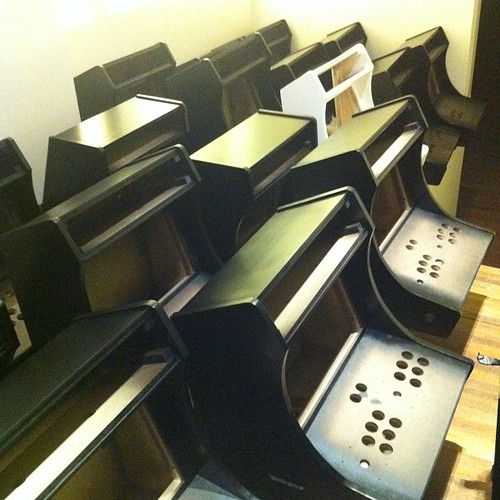
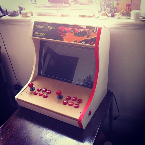
As visitors to my office have noticed, we’ve been building a bunch of arcade machines for clients.
Here are a couple of pics of the builds in progress:
Chassis’s undergoing painting
Unfinished machine
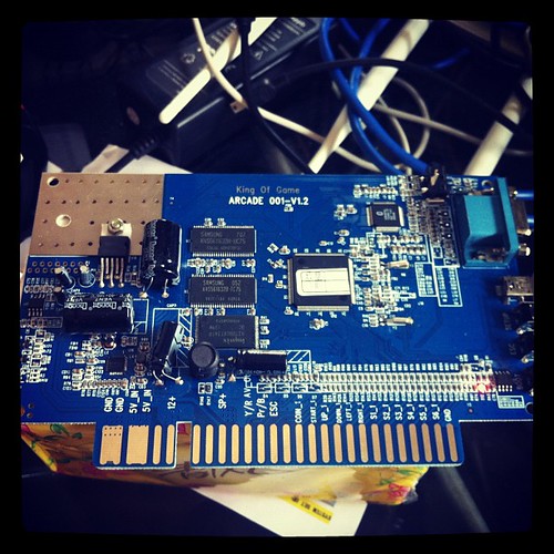
While making those is fun, I also have an interest in what powers them.
Arcade Machines are really just a wooden box, a display, a controller board, input (buttons and joysticks), and a PSU, they’re pretty basic devices. There is an industry cabling standard – JAMMA which makes connecting them up nice and easy.
China has a number of hardware choices for powering them, ranging from PC based boards, original arcade boards, and what I think is the better solution for older games – emulation under embedded ARM/MIPS, vs dedicated boards.
We went through a number of different versions of hardware available here until I found something I liked.
Our currently build hardware du jour runs off of something called “King of Game”.
As is usual in China, no documentation, and the factory is less than forthcoming with information.
Still, not unusual.
The device does have some interesting features for the would be hacker –
It has a nicely labelled “Boot” button, and the component count is quite low. Which generally means its SoC (System on a Chip) based.
The factory has done a little bit of prep work in making sure us ev1l hackorz won’t get at the juicy bits by etching off the cpu.
A quick look at the chip pin count, and the usual choice of chipset SoC more or less got me the right answer in a few minutes though.
My guess was Ingenic 4850, and it turned out to be the Ingenic 4755. This is a MIPS based X-Burst CPU
Even though they’re Chinese vendor, Ingenic does a great job in providing readily available information about their chipset(s). Kudos to the Ingenic guys in Beijing for being so open!
Datasheets for the 4755 and more importantly toolchains are readily available at the Ingenic FTP site – ftp://ftp.ingenic.cn/2soc/4750
Back to the board.
The King of Game board has USB onboard.
Plugging it into a computer shows the flash files available, but unfortunately not the firmware bits I need to see / change (e.g. to upgrade emulator capabilities, and change graphics).
If I hold down boot and plug in the USB, I get prompted for the Ingenic 4750 drivers.
Those are relatively easy to find on the ingenic site, so get a hold of those yourselves.
In order to connect to the board, you use a USB_BOOT.exe (there are also Linux tools available).
I downloaded usbboot-1.4b usbboot1.4b-tools, and unzipped that.
The USB Boot file needs a config file though – and the default config files supplied didn’t work 🙁
So, off to check what could be up.
The USB_Boot utility requires a bunch of settings in order to communicate with a board. After a bit of fiddling playing around with possible options I got it talking to the board.
While I’m not certain I have the settings completely correct here is what I have right now:
[PLL]
EXTCLK 24 ;Define the external crystal in MHz
CPUSPEED 336 ;Define the PLL output frequency
PHMDIV 3 ;Define the frequency divider ratio of PLL=CCLK:PCLK=HCLK=MCLK
BOUDRATE 57600 ;Define the uart boudrate
USEUART 0 ;Use which uart, 0/1 for jz4740,0/1/2/3 for jz4750
[SDRAM]
BUSWIDTH 16 ;The bus width of the SDRAM in bits (16|32)
BANKS 4 ;The bank number (2|4)
ROWADDR 12 ;Row address width in bits (11-13)
COLADDR 9 ;Column address width in bits (8-12)
ISMOBILE 0 ;Define whether SDRAM is mobile SDRAM, this only valid for Jz4750 ,1:yes 0:no
ISBUSSHARE 1 ;Define whether SDRAM bus share with NAND 1:shared 0:unshared
[NAND]
BUSWIDTH 8 ;The width of the NAND flash chip in bits (8|16|32)
ROWCYCLES 3 ;The row address cycles (2|3)
PAGESIZE 2048 ;The page size of the NAND chip in bytes(512|2048|4096)
PAGEPERBLOCK 64 ;The page number per block
FORCEERASE 0 ;The force to erase flag (0|1)
OOBSIZE 64 ;oob size in byte
ECCPOS 6 ;Specify the ECC offset inside the oob data (0-[oobsize-1])
BADBLACKPOS 0 ;Specify the badblock flag offset inside the oob (0-[oobsize-1])
BADBLACKPAGE 127 ;Specify the page number of badblock flag inside a block(0-[PAGEPERBLOCK-1])
PLANENUM 1 ;The planes number of target nand flash
BCHBIT 4 ;Specify the hardware BCH algorithm for 4750 (4|8)
WPPIN 0 ;Specify the write protect pin number
BLOCKPERCHIP 0 ;Specify the block number per chip,0 means ignore
[END]
If I put the board into USB boot mode (hold down boot button, and plug into the usb), then run the USB_TOOL.EXE file I can communicate
 Welcome!

 USB Boot Host Software!

 USB Boot Software current version: 1.4b

 Handling user command.

 USBBoot :> list
Device number can connect :1
USBBoot :> help
Command support in current version:
help print this help;
boot boot device and make it in stage2;
list show current device number can connect;
fconfig set USB Boot config file;
nquery query NAND flash info;
nread read NAND flash data with checking bad block and ECC;
nreadraw read NAND flash data without checking bad block and ECC;
nreadoob read NAND flash oob without checking bad block and ECC;
nerase erase NAND flash;
nprog program NAND flash with data and ECC;
nmark mark a bad block in NAND flash;
go execute program in SDRAM;
version show current USB Boot software version;
exit quit from telnet session;
readnand read data from nand flash and store to SDRAM;
load load file data to SDRAM;
run run command script in file;
memtest do SDRAM test;
gpios let one GPIO to high level;
gpioc let one GPIO to low level;
sdprog program SD card;
sdread read data from SD card;
USBBoot :> boot
Usage: boot (1)
1:device index number
USBBoot :> boot 0
Checking state of No.0 device: Unboot
Now booting No.0 device:
Download stage one program and execute at 0x80002000: Pass
Download stage two program and execute at 0x80c00000: Pass
Boot success!
Now configure No.0 device:
Now checking whether all configure args valid:
Current device information: CPU is Jz4750
Crystal work at 24MHz, the CCLK up to 336MHz and PMH_CLK up to 112MHz
Total SDRAM size is 16 MB, work in 4 bank and 16 bit mode
Nand page size 2048, ECC offset 6, bad block ID 127, use 1 plane mode
Configure success!
Next up, read the firmware off the flash, and dump it to see which version of the Dingoo code they most probably ripped off 🙂
31
Kudelski N3 bits and pieces.
Kudelski N3 bits and pieces, plus thoughts on key / rsa extraction from flash.
N3 Notes mostly from forum posts by TheCoder
These are notes for future reference more than anything else, so please no excited emails about how its wrong, or right, or can I hack your box.
—
There are three different pairing methods used N3 boxes presently. These are DT06, DT08 and Secondary key.
The DT06 method transfers a compressed form of an rsa pq keyset from which the CAM public/private rsa keyset and its associated modulus can be derived.
The DT08 method transfers the cam modulus along with the IRD number of the married box. The public rsa key is not transferred but it is implied that the box already knows this value.
The Secondary key method does not involve a transfer. It imples that the box already knows the cards matching CAM modulus and rsa public key value.
Various boxes, depending on make/model, may use any of the above pre-pair key transfer methods but it could be useful to know which box uses which method.
http://www.digital-kaos.co.uk/forums/f10/people-n3-cards-82421/
Instructions:
1 Stick your N2/N3 card in your card reader
2 Run NagraEdit – DO NOT ATTEMPT TO READ YOUR CARD !!!
3 Select the Comm Tab. This should give you an upper and lower text pane
4 Cut/Paste the scriptt below into the top pane
5 Press the “Send D2C” button/icon
6 Results should appear in bottom pane
7 Interpret your results based on info below.
Script – Read DT06/DT08
Code:
rs
tx 21 C1 01 FE 1F
rx
tx 21 00 08 A0 CA 00 00 02 12 00 06 55
dl 02 00
rx
dl 02 00
tx 21 00 09 A0 CA 00 00 03 22 01 00 1C 7E
dl 02 00
rx
dl 02 00
mg *
mg *** DT06 info ***
tx 21 00 09 A0 CA 00 00 03 22 01 06 13 **
dl 02 00
rx
mg DT06 response1
dl 02 00
tx 21 40 09 A0 CA 00 00 03 22 01 86 13 **
dl 02 00
rx
dl 02 00
mg DT06 response2
mg *** End DT06 info ***
mg *
mg *** DT08 info ***
tx 21 40 09 A0 CA 00 00 03 22 01 08 13 **
dl 02 00
rx
mg DT08 response1
dl 02 00
tx 21 00 09 A0 CA 00 00 03 22 01 C8 55 **
dl 02 00
rx
dl 02 00
mg DT08 response2
tx 21 40 09 A0 CA 00 00 03 22 01 88 55 **
dl 02 00
rx
mg DT08 response3
dl 02 00
mg *** End DT08 info ***
*******
Just to clarify :
The important bits your looking at are the DT06/DT08 responses (the bits that start with Rx: )
ie RX: 12 00 15 A2 11 08 E0 00 00 00 5E 01 20 00 00 00
00 00 00 00 00 00 90 00 B3
RX: 12 40 15 A2 11 00 00 00 00 00 00 00 00 00 00 00
00 00 00 00 00 00 90 00 64
RX: 12 00 15 A2 11 00 00 00 00 00 00 00 00 00 00 00
00 00 00 00 00 00 90 00 24
and
RX: 12 40 57 A2 53 00 00 00 00 00 00 00 00 00 00 00
00 00 00 00 00 00 00 00 00 00 00 00 00 00 00 00
00 00 00 00 00 00 00 00 00 00 00 00 00 00 00 00
00 00 00 00 00 00 00 00 00 00 00 00 00 00 00 00
00 00 00 00 00 00 00 00 00 00 00 00 00 00 00 00
00 00 00 00 00 00 00 00 90 00 64
If the responses vary significantly from the above, with the 00’s replaced with some varying data, then its likely your card had the specified tier and is probably using the corresponding pairing method.
If the DT06 response contains lots of 00’s then its NOT DT06 pairing
If the DT08 response contains lots of 00’s then its NOT DT08 pairing
If its not DT06 or DT08 then its probably secondary key.
For non DT08 cards (mostly the newer boxes) each box has a unique cam_n already built into its firmware – this can only be extracted from the actual box itself.
About the Algorithm,
N2 encrytion was based on the following algorithm ->
decrypted message = ( (IDEA( ( (EncryptedMsg ^ 3)Mod N1) ,IdeaKey) ) ^3) Mod N1
Thats 2 distinct algorithms. An RSA algorithm (performed twice) and an IDEA algorithm.
The key for the RSA algorithm is something like –
RSA EMM-G=15A811B2065DF39CD48C9C958E7B406345295B09D0E9A18A 9B92C5FD7761CAAFAB830880F1F06B4E4477F157EA10D0AFC3 FDDB1ED2E7E83E89F03FF81237047DB76F79D6A2CFD75A7255 D72E52E7F47B96C2DFBDEBFC80CE927F6AD351FDF0BF8DA13F F62295BFBAF29035A230136D0B4AA99D38DD8B0465F2C709FC 8818173C
Which, as you can see, is a 128 byte (1024 bit) number. This is the main encryption key for EMM decryption.
The IDEA algorithm, which acts as an inner layer to the RSA has a standard 16 byte (128 bit) IDEA key.
There is no algorithm in N2 (or N3) that only uses an 8 byte (64 bit) key although some providers have opted to use 3DES rather than IDEA as an inner layer. This uses three separate 8 bye (64 bit – only 56 bits used) keys to form an amalgam 168 bit DES algorithm.
If Using DT08 (0a) on the card :
The Dt08 (0a datatype on card) is created by the provider and sent to the card at sub time.
The dt08 contains the Cam N public rsa key along with ird/boxkey.
The dt08 is IDEA encrypted with the Idea Key made from ird/boxkey/inverted ird.
The dt08 is RSA encrypted using Ird N (public rsa key) and Ird D (private key and uknown by anyone but provider).
Ird N = N1 xored N2
Ird N1= A4E9B585932F90282FD70C908176E8605E6B2CE629335A0FC1 5B31DAB0BFC6FEEB88CFC69649994CD3FE039C9965C620C4D5 828E9153998EE4AE0E8C25644DF3 xor
Ird N1= 237280AAB36BE4B21FC71FBF08218E532A545E744D7B007FF8 69BA426831C4AC653F3825ADE9358FCD1F0239EC447CBC2765 CC0AEBE437AF2270FC461C2FA042
Ird N = 879B352F2044749A3010132F89576633743F729264485A7039 328B98D88E02528EB7F7E33BA0ACC31EE101A57521BA9CE3B0 4E847AB7AE21C6DEF2CA394BEDB1
The Ird N1,N2,Ideakey exist in the tsop.
Ird E = 3
Ird D = UKNOWN, this is the reason you can’t create your own dt08 without changing the N1/N2 on the tsop, you must know Ird D.
DT08 (0A) = IdeaEncrypt(CamN/Ird#/Boxkey/Idea Signature,Ird_Ideakey) ^ D mod Ird N.
Ird requests DT08.
Card sends back the dt08 (0a)
Ird decrypts the dt08.
Decrypted dt08 = IdeaDecrypt(DT08,Ird_IdeaKey) ^ 3 mod Ird N.
It checks the ird # and boxkeys in the Decrypted 08 if they match what is on ird,
it stores the Cam N in the decrypted 08 in ird memmory.
If Using Secondary Key (SK) on the Ird.
Ird checks for SK exists on the ird, if it does, the dt08 will never be requested/ignored from the card.
Ird validates the SK with idea signature in the SK (using IIIIIIII01924314051647990A9C4E1 where I = irdnumber).
Ird takes the Cam N in the SK and puts it in ird memmory
Note : Cam N is not even encrypted in the sk, very weak method compared to dt08.
Later, establish session key (0C datatype on the card):
Ird requests 2a data from card.
Random 2a is sent from card to ird.
Ird performs some Idea signing (leave it to you to look up 2a/2b routines)
Ird comes up with session key from the 2a message sent from Cam.
Ird encrypts the session key with rsa.
Encrypted 2B = (2B data with 16 byte session idea key) ^ 3 mod Cam N.
Sends encrypted data back to card in 2b message.
Cam decrypts 2B with Cam N, Cam D. Decrypted 2B = (Encrypted 2B) ^ Cam D mod Cam N.
If valid, store session key in ram and on card for later use.
This all happens as ird boots.
When you select a channel.
Ird sends Cmd 07 ECM message with control words encrypted.
Cam decrypts the control words rencrypts them with Idea encryption using the session key established above.
The ird then requests the control words.
The Cam sends them back in the 1C response.
The ird decrypts the control words with with Idea encryption using the session key established above.
Sends the control words to the mpeg decoder.
8 seconds of video.
Repeat 07/1C process over and over.
——–
and pay special attention on CMD$2A ??
it should reply the CAMID serial number + 64 bytes random key generated and then shortly after encrypted with the CAM(AKA Conditional Access Module or SmartCard) RSA primary 96 bytes from the card… the so famous RSA modulus keys 96bytes at eeprom $8xxx on the ROM110 days.. From the card (this cmd is also the first step of the SessionKey negotiation)
shortly after the receiver receives this card reply.. and will decrypt it using the Secondary Key which is also 96bytes, this key is build up by using the following information stored in the receivers flash..
IR IR IR IR ZZ ZZ ZZ ZZ ZZ ZZ ZZ ZZ 00 03 F1 F1
F1 F1 F1 F1 F1 F1 SK SK SK SK SK SK SK SK SK SK
SK SK SK SK SK SK SK SK SK SK SK SK SK SK SK SK
SK SK SK SK SK SK SK SK SK SK SK SK SK SK SK SK
SK SK SK SK SK SK SK SK SK SK SK SK SK SK SK SK
SK SK SK SK SK SK F2 F2 F2 F2 F2 F2 F2 F2 CR CR
total 96 bytes..
IR = Receiver serial number
XX = Unimportant
EE = RSA public exponent for STB
F1 = SK signature 1 used to calculate the box key
F2 = SK signature 2 used to calculate the box key
SK = RSA public modulus N
CR = CRC Checksum
BB = BoxKey result from xoring F1 with F2 keys stored in the flash firmware from the receiver
once we decrypt the cmd2A we extract from inside the original 64byte random key generated in the card, then we will apply the IDEA encryption algo on the first 32bytes from the 64 byte random key to hash out the session key.
So this first 32 bytes are extracted from the 64byte random key and will be encryted using the IDEA SIGNATURE key… this key will be generated by the following information
IdeaKey generation
BB BB BB BB BB BB BB BB + CC CC CC CC + CA MI DC AM
BBBBBBBBBBBBBBBB = Boxkey result from F1 xor F2
CCCCCCCC = IRD number from receiver stored in Flash firmware
CA MI DC AM = CAM ID or Smart Card serial number converted in HEX, which can also be extracted by simply sending INS CMD$12 to the card..
so the IDEA signature key for encrypting the first 32bytes extracted from the 64 random seek key is
BBBBBBBBBBBBBBBBCCCCCAMIDCAM
once applied the IDEA encryption we will have the result 16 byte sessionkey.. which will be stored in the receiver flash for a few hours… to be more precise around 5 hours..
Now going back to the calculation done before, the receiver decrypted the cmd$2Aencrypted by the card with the RSA primary 96 stored in the card.
once decrypted it simply just extracted the first 32bytes of the 64 byte seed key generated by the card. this 32 bytes were used for calculation of the 16byte sessionkey..
but, before the 32byte keys was taken for the idea signature encryption.. the receiver.. re-encrypted the 64byte random key using the SECONDARY KEY RSA 96 stored in the receiver flash, which i just stated above how to get this key…
and will send it back to the card on cmd$2B
the card will receive the cmd$2b and will decrypt it using the PRIMARY RSA modulus key 96.
and will extract just the first 32bytes.. and by using the BOXKEY+IRD+CAMID stored in the card, the card will also calculate the same 16 byte session key.
in orde to make the card pairing , u need to know the RSA_N+BOXKEY+IRD NUMBER+CARD SERIAL number or CAMID…
then with them all together we can start comunication between the card.. and on the CMD$2A and $2B we will have the SessionKey negotiation which i just explained previously.
if for example on one side or the other we have different BKand RSA… we will a session key failure.. and without this Sessionkey we will not be able to decrypt the CM$1C or $9C related stuff
this means that if negotiation of session key succeds, then the receiver will send the ECM$07 to the card, which will then be decrypted by simply just using the ECM RSA modulus key and the ECM IdeaKey to decrypt the Control Words / CWs.
once they are decrypted the card will send them to the RECEIVER.. this is normally done via CMD$1C obviously this CMD is encrypted with the Sessionkey 16 BYTES described above.. once it arrives at the Receiver end, you will use the same Sessionkey 16byte to decrypt that CMD$1C and extract the REAL DCWs Decrypted Control Words to open up the Video and Audio stream related for that XX amount of seconds…
Now this Session key is refreshed every 5 hours.. this means that every 5 hours a new session key is produced.. so every 5 hours the card generates another 64byte random seed key using other RSA algo inside the card.., and will then send this 64 byte seed key to the receiver again.
Shortly followed by all the procedure described above to extract the new session key again.
—————-
Given that ==================================================
SK 96 BYTES
==================================================
11111111<----------------------------FIRST 4 BYTES---- IRD
XXXXXXXXXXXXXXXXXXXX<--NEXT 10 BYTES---- unknown
1111111111111111<--------8 BYTES---- Y1---WRITE DOWN
==================================================
11111111111111111111111111111111-_
11111111111111111111111111111111-_-_"N" 64 Bytes
11111111111111111111111111111111-_-
11111111111111111111111111111111-
==================================================
1111111111111111<-------8 BYTES--- Y2-----WRITE DOWN
XXXX<-------------------2 BYTES--- CHECKSUM
==================================================
Y2 Xor Y1 = BOXKEY
==================================================
006e convert from hex gives you 110 bytes block cipher
ird 4 bytes
bk 8 bytes
sk 96 bytes
leaving us with 02bytes used to encrypt, decrypt above.
eg:
00 00 00 6e 34 0d 20 1c 03 03 70 80 5a 8e dd 24
ac cc a4 a6 e2 da 86 91 29 18 0b a6 23 6d fa c4
05 7f 1b 20 97 eb 0c 19 b3 39 2f 1e cb 9b 67 4d
ed 10 f5 65 ec 0d c7 35 ac f0 b8 89 b0 51 59 22
69 85 d5 f1 93 48 7a 84 6e 1f b4 24 83 79 db 02
4d b0 9c 5e 8b df 89 57 9c 5a 7f 9a cc 87 51 3b
15 6b 15 cc c4 2f 66 e7 e6 75 4f 24 f2 07 85 0d
db b0 3d e2 64 dd e9 54 ad 77 60 e7 8f a6 cd a6
46 c3 b8 fa e4 e7 51 2d 6a 2f 95 68 56 b5 78 34
17 6b b8 48 38 87 c4 95 e5 b0 41 2c 95 e1 24 aa
4b 2a 6f 8c 90 53 29 a9 6b 3d 0a b5 92 1c 95 ec
72 b9 54 a9 99 f5 f3 dd f4 0f 60 c3 25 5b 5b 81
22 e8 79 c5 be 8f 3c 89 2b 8a ad ba 27 b0 c2 f7
b1 4f 08 d5 37 2a 97 c5 f0 07 9d 99 be c7 8a a9
cf 5a c5 45 ce 1e 25 43 81 95 7a 22 33 ed 93 74
Gives:
00 00 00 63 (length)
0d 20 1c 03 03 70 80 5a 8e dd (unknown)
24 ac cc a4 a6 e2 da 86 (y1)
91 29 18 0b a6 23 6d fa c4
05 7f 1b 20 97 eb 0c 19 b3 39 2f 1e cb 9b 67 4d
ed 10 f5 65 ec 0d c7 35 ac f0 b8 89 b0 51 59 22
69 85 d5 f1 93 48 7a 84 6e 1f b4 24 83 79 db 02
4d b0 9c 5e 8b df 89 (64 bytes)
57 9c 5a 7f 9a cc 87 51 (y2)
Y2 XOR Y1 = 0x579c5a7f9acc8751 xor 0x24accca4a6e2da86 = 42 12 8C F2 39 39 55 FA
So, a flash dump would be helpful..
Possible Scenario's -
BGA, TSOP, TLGA etc.. desoldering for Flash.
Put in a socket. eg from
http://shop37051047.taobao.com/ or http://shop34694309.taobao.com/?search=y
Pop flash back onto something else, read, dump. eg
http://item.taobao.com/item.htm?id=7422440993
Get box key, rsa key (if req. based on a check of DT type from the actual subbed card)
Pop flash back in socket.
Been there, done that for data recovery on faulty flash drives, plus most of the places I know down at QJlu have SMD / BGA desoldering capability or better.
Bunnies blog is fairly good at explaining the basics (albeit for xbox) – http://www.xenatera.com/bunnie/proj/anatak/xboxmod.html
Most boxes use ARM based SoC’s for things. Also possible to just throw up a dev board, and interface to that.
Although most boxes also have some form of OS running, so just as feasible to dump flash that way also assuming serial or jtag access and a bootloader is available.
Amusing that people like http://www.flashbackdata.com/blog/?p=195 claim this is hard – there are plenty of tools for this already out there eg softcenter, pc3000, plus all the local chinese stuff. Semi ok forum here talking about flash recovery, although not as technical as I’d like.
http://forum.hddguru.com/hard-disk-drives-english-forum-f12.html
Once key(s) are had, then I can use my own decoder rather than the crappy one the broadcaster uses.
Yay.
Archives
- November 2024
- November 2019
- October 2019
- August 2019
- April 2019
- February 2017
- September 2016
- June 2016
- May 2016
- September 2015
- August 2015
- June 2015
- April 2015
- December 2014
- October 2014
- September 2014
- July 2014
- June 2014
- April 2014
- October 2013
- July 2013
- May 2013
- April 2013
- March 2013
- January 2013
- December 2012
- October 2012
- August 2012
- July 2012
- June 2012
- May 2012
- April 2012
- March 2012
- December 2011
- November 2011
- October 2011
- September 2011
- July 2011
- May 2011
- April 2011
- March 2011
- February 2011
- January 2011
- December 2010
- November 2010
- October 2010
- September 2010
- August 2010
- July 2010
- June 2010
- May 2010
- April 2010
- March 2010
- February 2010
- January 2010
- December 2009
- November 2009
- October 2009
- May 2009
- April 2009
- March 2009
- February 2009
- January 2009
- December 2008
- November 2008
- October 2008
- September 2008
Categories
- Apple
- Arcade Machines
- Badges
- BMW
- China Related
- Cool Hunting
- Exploits
- Firmware
- Food
- General Talk
- government
- IP Cam
- iPhone
- Lasers
- legislation
- MODx
- MySQL
- notice
- qmail
- requirements
- Reviews
- Service Issues
- Tao Bao
- Technical Mumbo Jumbo
- Things that will get me censored
- Travel
- Uncategorized
- Useful Info