Someone from the JammaForums.co.uk emailed me a copy of the firmware in their SD card from a XinYe 138 in 1.
Card looks something like this:

I don’t have one, but I took a quick look at the data provided, and it looks fairly straightforward to “hack”.
It actually took me less than 30 minutes to have most of the good bits extracted from receiving the file!
There are 2 files on the SD card.
One is a 64 byte file called sn.bin which contains this data:

This looks suspiciously like a header, but I haven’t taken a clear look.
The second file is called x3rodl.bin, and contains a Linux firmware in ARM format.
The first few hundred bytes look like this:

Its obviously in ARM format, as the first set of bytes are ARM no-op codes.
00 00 A0 E1, which repeats 8 times.
02 00 00 EA, then…
18 28 6F 01 – Which is a magic word indicating that this contains a zImage (compressed Linux kernel)
18 28 6F 01 = 0x016f2818
Linux code looks something like this for identifying if its a kernel:
if (*(ulong *)(to + 9*4) != LINUX_ZIMAGE_MAGIC) {

        printk("Warning: this binary is not compressed linux kernel image/n");

        printk("zImage magic = 0x%08lx/n", *(ulong *)(to + 9*4));

    } else {

        printk("zImage magic = 0x%08lx/n", *(ulong *)(to + 9*4));

    }
9 * 4 = 36, which is our location, and this happens to have our magic number.
So, we know its a kernel. Its also probably the VIVI bootloader from Samsung, as that uses that style MAGIC.
The following bits of data, contain the setup for the kernel, and the boot code.
This continues on until the compressed kernel+ramdisk. That starts with 1F 8B 08 (gzip header bytes) over at 0x3EF2, until roughly the end of the file.
I extracted that part and had a quick look.
Its about 7.7M size unpacked.
Linux version is: 2.6.36-FriendlyARM
Boot params are:
console=ttySAC0,115200 root=/dev/ram init=/linuxrc initrd=0x51000000,6M ramdisk_size=6144
RAMDISK File System starts at 0x20000, and looks like this:
lawrence$ ls -al

total 24

drwxr-xr-x  13 lawrence  staff   442 Jun 17 23:09 .

drwxr-xr-x   4 lawrence  staff   136 Jun 17 23:08 ..

drwxr-xr-x  51 lawrence  staff  1734 Jun 17 23:09 bin

drwxr-xr-x   2 lawrence  staff    68 Jun 17 23:09 dev

drwxr-xr-x  11 lawrence  staff   374 Jun 17 23:09 etc

-rwxr-xr-x   1 lawrence  staff  3821 Jun 17 23:09 init

-rw-r--r--   1 lawrence  staff  3821 Jun 17 23:09 init~

lrwxrwxrwx   1 lawrence  staff    11 Jun 17 23:09 linuxrc -> bin/busybox

drwxr-xr-x   2 lawrence  staff    68 Jun 17 23:09 proc

drwxr-xr-x   2 lawrence  staff    68 Jun 17 23:09 r

drwxr-xr-x  19 lawrence  staff   646 Jun 17 23:09 sbin

drwxr-xr-x   2 lawrence  staff    68 Jun 17 23:09 sdcard

drwxr-xr-x   4 lawrence  staff   136 Jun 17 23:09 usr
The bootup script for this looks like this:
#! /bin/sh
PATH=/sbin:/bin:/usr/sbin:/usr/bin
runlevel=S
prevlevel=N
umask 022
export PATH runlevel prevlevel
echo st.
#
# Trap CTRL-C &c only in this shell so we can interrupt subprocesses.
#
trap ":" INT QUIT TSTP
/bin/hostname FriendlyARM
/bin/mount -n -t proc proc /proc
cmdline=`cat /proc/cmdline`
ROOT=none
ROOTFLAGS=
ROOTFSTYPE=
NFSROOT=
IP=
INIT=/sbin/init
#run_fs_image=/images/linux/rootfs_xin1arm_sdhotplug.ext3
for x in $cmdline ; do
case $x in
root=*)
ROOT=${x#root=}
;;
rootfstype=*)
ROOTFSTYPE="-t ${x#rootfstype=}"
;;
rootflags=*)
ROOTFLAGS="-o ${x#rootflags=}"
;;
init=*)
INIT=${x#init=}
;;
nfsroot=*)
NFSROOT=${x#nfsroot=}
;;
ip=*)
IP=${x#ip=}
;;
esac
done
if [ ! -z $NFSROOT ] ; then
echo $NFSROOT | sed s/:/\ /g > /dev/x ; read sip dir < /dev/x
echo $IP | sed s/:/\ /g > /dev/x; read cip sip2 gip netmask hostname device autoconf < /dev/x
rm /dev/x
#echo $sip $dir $cip $sip2 $gip $netmask $hostname $device $autoconf
mount -t nfs $NFSROOT /r -o nolock,proto=tcp
#[ -e /r/dev/console ] || exec /bin/sh
elif [ ! -z $run_fs_image ] ; then
#lilxc
#echo $run_fs_image
echo sdroot.
if [ ! -e /dev/mmcblk0p2 ] ; then
echo "p2 not found."
reboot
sleep 5
fi
ROOTFSTYPE="-t ext3"
for i in 1 2 3 4 5 ; do
#/bin/mount -n -o sync -o noatime -o nodiratime -o ro -t vfat /dev/mmcblk0p1 /sdcard && break
/bin/mount -n -o sync -o noatime -o nodiratime -o ro -t ext3 /dev/mmcblk0p2 /sdcard && break
echo Waiting for SD Card...
if [ $i = 4 ] ; then
echo " p2 failed. "
reboot
sleep 5
break;
fi
sleep 1
done
#echo ------begin----------------------------------------
#sleep 1
#lilxc
#ls -l /dev
#sleep 1
#echo -----------------------------------------------
#ls -l /sdcard
#sleep 1
#echo ------end------------------------------------------
#/sbin/losetup /dev/loop0 /sdcard/$run_fs_image
#/bin/mount $ROOTFSTYPE /dev/loop0 /r
#/bin/mount $ROOTFSTYPE -o noatime -o nodiratime -o ro /dev/mmcblk0p2 /r > /dev/null 2>&1
/bin/mount $ROOTFSTYPE -n -o noatime -o nodiratime -o ro /dev/mmcblk0p3 /r > /dev/null 2>&1
mount -o move /sdcard /r/sdcard
#/sbin/losetup /dev/loop1 /r/sdcard/swap
#/sbin/swapon /dev/loop1
else
# /bin/mount -n $ROOTFLAGS $ROOTFSTYPE $ROOT /r
# echo "Readonly mount...(lilxc)"
# mount -n -t yaffs2 -o noatime -o nodiratime -o ro /dev/mtdblock2 /r
# mount -n -t yaffs2 -o noatime -o nodiratime /dev/mtdblock2 /r
mount -n -t yaffs2 -o noatime -o nodiratime -o ro /dev/mtdblock2 /r
if [ -e /r/home/plg/reboot ]; then
umount /r
mount -n -t yaffs2 -o noatime -o nodiratime /dev/mtdblock2 /r
fi
fi
ONE_WIRE_PROC=/proc/driver/one-wire-info
ETC_BASE=/r/etc
[ -d /r/system/etc ] && ETC_BASE=/r/system/etc
[ -e $ETC_BASE/ts.detected ] && . $ETC_BASE/ts.detected
[ -z $CHECK_1WIRE ] && CHECK_1WIRE=Y
if [ $CHECK_1WIRE = "Y" -a -e $ONE_WIRE_PROC ] ; then
if read lcd_type fw_ver tail < $ONE_WIRE_PROC ; then
if [ x$lcd_type = "x0" -a x$fw_ver = "x0" ] ; then
TS_DEV=/dev/touchscreen
else
TS_DEV=/dev/touchscreen-1wire
echo "1Wire touchscreen OK"
fi
if [ -e $ETC_BASE/friendlyarm-ts-input.conf ]; then
sed "s:^\(TSLIB_TSDEVICE=\).*:\1$TS_DEV:g" $ETC_BASE/friendlyarm-ts-input.conf > $ETC_BASE/ts-autodetect.conf
mv $ETC_BASE/ts-autodetect.conf $ETC_BASE/friendlyarm-ts-input.conf -f
echo "CHECK_1WIRE=N" > $ETC_BASE/ts.detected
fi
fi
fi
[ -e /r/etc/friendlyarm-ts-input.conf ] && . /r/etc/friendlyarm-ts-input.conf
[ -e /r/system/etc/friendlyarm-ts-input.conf ] && . /r/system/etc/friendlyarm-ts-input.conf
export TSLIB_TSDEVICE
#lilxc debug here
#/bin/mount -n -o sync -o noatime -o nodiratime -t vfat /dev/mmcblk0p1 /sdcard
#cp /sdcard/lktcmd /r/tmp
#exec /bin/sh
# for running game
umount /proc
exec switch_root /r $INIT /r/dev/console 2>&1
The secondary loader in init looks like this:
#! /bin/sh
PATH=/sbin:/bin:/usr/sbin:/usr/bin:/usr/local/bin:
runlevel=S
prevlevel=N
umask 022
export PATH runlevel prevlevel
#
# Trap CTRL-C &c only in this shell so we can interrupt subprocesses.
#
trap ":" INT QUIT TSTP
/bin/hostname FriendlyARM
[ -e /proc/1 ] || /bin/mount -n -t proc none /proc
[ -e /sys/class ] || /bin/mount -n -t sysfs none /sys
[ -e /dev/tty ] || /bin/mount -t ramfs none /dev
/bin/mount -n -t usbfs none /proc/bus/usb
echo /sbin/mdev > /proc/sys/kernel/hotplug
/sbin/mdev -s
/bin/hotplug
# mounting file system specified in /etc/fstab
mkdir -p /dev/pts
mkdir -p /dev/shm
/bin/mount -n -t devpts none /dev/pts -o mode=0622
/bin/mount -n -t tmpfs tmpfs /dev/shm
/bin/mount -n -t ramfs none /tmp
/bin/mount -n -t ramfs none /var
mkdir -p /var/empty
mkdir -p /var/log
mkdir -p /var/lock
mkdir -p /var/run
mkdir -p /var/tmp
/sbin/hwclock -s
echo " " > /dev/tty1
echo "System starting... " > /dev/tty1
syslogd
#/etc/rc.d/init.d/netd start
#echo " " > /dev/tty1
#echo "Starting networking..." > /dev/tty1
#sleep 1
#/etc/rc.d/init.d/httpd start
#echo " " > /dev/tty1
#echo "Starting web server..." > /dev/tty1
#sleep 1
#/etc/rc.d/init.d/leds start
#echo " " > /dev/tty1
#echo "Starting leds service..." > /dev/tty1
#echo " "
#sleep 1
/etc/rc.d/init.d/mkjoy
#echo " " > /dev/tty1
#echo "System Starting... " > /dev/tty1
#echo " " > /dev/tty1
#echo " " > /dev/tty1
/etc/rc.d/init.d/alsaconf start
#echo "Loading sound card config..." > /dev/tty1
#echo " "
#/sbin/ifconfig lo 127.0.0.1
#/etc/init.d/ifconfig-eth0
#/bin/qtopia &
#echo " " > /dev/tty1
#echo "Starting Qtopia, please waiting..." > /dev/tty1
cd /sdcard
./run.sh
reboot
Fairly easy to reverse!
Refs:
http://www.jammaplus.co.uk/
http://blog.csdn.net/liangkaiming/article/details/6259189
Following up from my previous posts on this, looks like my idea’s are correct about the size of the NAND for setup, and my NAND read stuff works. Yay for me.
Lets recap:
JZ4755 boot sequence is as follows:
CPU powers up.
Checks BOOT_SEL line, takes appropriate action.
boot_sel[1:0]

00	Unused

01	Initialization via USB port: Receives a block of data through the USB (device) port,

and stores it in internal SRAM.

10	Initialization via NAND memory with 512-byte pages at Chip Select 1 (CS1):

11	Initialization via NAND memory with 2048-byte pages at Chip Select 1 (CS1):
In our board, if we press BOOT, this pulls the pin low, so CPU see’s 01, and waits for an IPL from USB.
If we leave it to boot normally, then it reads from NAND.
So far so good.
Lets see if anyone was watching carefully 🙂
Our board NAND chip has a page size of 8192+OOB
Our *CPU Hardware* supports either 512bytes or 2048bytes page size on boot.
Our IPL (aka NAND.BIN) must be 8K in size or less, as the CPU has 8k only, and it copies the bootloader to that obeying BOOT_SEL.
Lets look at what happens.
If I read out the NAND (NREAD 0 8192 0 0) with our carefully set sizing, I see the following:
0000 - 2047 (2k in size) -  DATA  FF 55 55 .. 02 00 0C

2048 - 2549 (512bytes in size)  - BLANK

2560 - 4607 (2k in size) - DATA (padded at end with FF's to 2k size) 21 20 00 .. 85 8c 90+ FF -> 2048 end

4608 - 6655 (2k in size) - DATA  (padded at end with FF's to 2k size)
So, we have roughly about 6k odd of data, out of our 8k max. Its a bit weirdly laid out though, and has some holes in there, so its _not_ correct 🙁
Lets look at the RAW NAND DUMP (NREAD_RAW 0 8192 0 0). Our raw page size is 8192.
Page 0

00000 - 02047 (2k in size) - DATA  FF 55 55 .. 02 00 0C (same as before)

02048 - 02102 (55 bytes)   - (presumed OOB / ECC stuff...) NEW

Page 1

08192 - 10239 (2k in size) - DATA 21 20 00 .. 10 80 00.  Our 85 8c 90 above is actually part of the 55byte sequence, so definitely our NREAD is incorrect, as we're suddenly short data.

10240 - 10294 (55 bytes )  - (presumed OOB / ECC stuff...) NEW

Page 2

16384 - 18431 (2k in size) - DATA (padded with 0's from 17892 - 18431), so our NAND loader data is roughly 5.5KBish.

18432 - 18486 (55 bytes )  - (presumed OOB / ECC stuff...) NEW

Page 3

25026 onwards FF's - so uninitialized.
So, with that, we know that NREAD doesn’t quite work for our first 4 pages (page 0 – 3), and we either need to NREAD_RAW, or possibly use a 2048byte page size in order to read the NAND.BIN properly.
Thats only necessary for the first 4 pages in the NAND though.
Once the NAND.BIN MINIOS bootstrap is running, it should be able to cope with our proper data size.
How does it do that though?
MINIOS Bootloader starts up, as it gets added to the CPU boot sequence detailed above, then it looks for 3 things in 3 places 🙂
Our mystery locations for that are:
Page 61
Page 62
Page 63
Page 61 contains our NAND size stuff, which as we know from above, our Bootloader *can’t* use, as its only 2k or 512byte set at the hardware level initially.
Page 61 in mine has 12 bytes. This looks exceedingly good as I know that my work is, er, working 🙂
USBBoot :> nreadraw 61 24 0 0

Reading RAW from No.0 device No.0 flash....

0x00000000 :00 20 00 00 c0 01 00 00 00 01 00 00
00 20 00 00 = 8192 PAGE SIZE
c0 01 00 00 = 448 OOBSIZE
00 01 00 00 = 256 PAGE PER BLOCK
Lets look at the 3 bytes.
First 16bit word is = 8192 – thats our Page Size
Second 16bit word is = 448 – thats our OOB size (oob = out of block, usually used for CRC or Error etc, as NAND can go BAD if you write to it frequently)
Third 16bit word is = 256 – thats how many pages per block we have.
Block 61, and Block 62 are the same. Basically 62 is a backup of 61. If the NAND.BIN MINIOS loader can’t read Block 61 12 bytes, it tries Block 62. If neither work, you’ll need to reflash, or replace the NAND…
Block 63 contains a whole 10 bytes. This is the UID of the device. Mine is set to 0. Lazy buggers 🙂
Ok, so now we booted, and the MINIOS bootstraploader / NAND.BIN has read our NAND size, then what?
Well, you’ll need to disassemble the code to see (eg as part of my previous post), but essentially it calls the next thing in line.
This can be Linux, or something else. In the board, the OS used is MINIOS, so it loads something else – aka MINIOS.
MINIOS is actually uCOS-II – You can find details on that from Micrium, as they licence it out.
Ingenic has a custom version of uCOS-II for their board. uCOS-II is also a RTOS (Real Time OS).
You can read more on MINIOS here – http://en.wikipedia.org/wiki/MicroC/OS-II
Anyway, lets get back to work, and less chatter 🙂
NAND.BIN passes control onto whatever is sitting at Page 128 (this can be changed, but in the JAMMA board, and in the GameBox GBX-0001), the next loader is at Page 128.
As I don’t have much info on the MINIOS side, I got a lot of this info from other places. Mostly the MINIOS_CFG.INI in the Ingenic FTP Site, plus some gracious help from Joseba Epalza (thanks!) at www.zonadepruebas.com. He supplied a Gamebox dump, and asked me a few questions, which made me re-examine things, which was extremely useful as then I could bounce idea’s and findings off of someone else.
The Gamebox hardware and the Jamma hardware is extremely similar, so the NAND dump in both is good for both of us to double check each others work. Unfortunately, I don’t speak Portuguese Spanish, so we both relied on Google Translate to talk via email today, but we seem to be doing ok 🙂
Onto the tech side again, our secondary loader is, in MINIOS terms, called LOADER.BIN
This sits at Page 128
LOADER.BIN tries to read a file called DEF_BOOT.BIN for configuration settings, as that tells LOADER.BIN where the rest of the filesystem is!
In theory, Page 256 contains
DEF_BOOT.BIN
I need to go back and recheck that now, as my dumps are a bit messy, and I need to check on actual hardware, vs the many whoops I renamed that wrong files I now have messing up my desktop.
I also need to check if I need to read as 2k block size/or raw to get the correct data in these pages, as one place online says that the secondary bootloader (LOADER.BIN) also assumes 2k size.
Other bits:
IMG_BOOT.BIN – bootup code if used.
MINIOS.BIN – the OS.
RES.BIN – Resources used by MINIOS.BIN
The rest… (FAT16 Filesystem which is readable over USB via normal boot)
—
Ignoring my first 8k not quite correct dumped dumps + possibly borked secondary loader stuff, the rest of the data dump looks accurate.
I have what looks like RES.BIN stuff, I have a MINIOS, and I can see interesting things.
Interesting things below:
Dump pos 0x100200 - seems to have the RES.BIN filesystem in mine -
mobile_tv.bin
desktop.bin
udc_battery.bin
sysconfig.bin
toolsbox.bin
calendar.bin
ebook.bin
worldclock.bin
russblock.bin
fmradio.bin
recorder.bin
mp3_compress.bin
viewer.bin
jpgdec.bin
pngdec.bin
bmpdec.bin
gifdec.bin
AudioTag.bin <-- significant, means case sensitive
vplayer.bin
fplayer.bin
aplayer.bin
video.bin
alarm.bin
gameplay.bin
gba_lib.bin
nes_lib.bin
snes_lib.bin
md_lib.bin
ticru_lib.bin
dcDecoder.bin
dvEncoder.bin
dcdv.bin
mpcodecs_ad_liba52.bin
mpcodecs_ad_hwac3.bin
ffmpeg64.bin
ffmpeg_vd_mpegmisc.bin
ffmpeg_vd_mpegmisc2.bin
ffpmeg_vd_mpegvideo.bin
mpcodecs_vs_libmpeg2.bin
ffmpeg_vd_svq3.bin
mpcodecs_vd_realvid.bin
aux_task.bin
desktoplib_simplen.bin
desktoplib_drawer.bin
desktoplib_slide.bin
desktoplib_tradition.bin <- chinese traditional
desktoplib_arena.bin
desktoplib_diorama.bin
So, I know that that part is correct at least, as it really truly looks like proper data 🙂
Other things of note.
Our FAT part of the NAND, that is USB accessible is referred to internally as nfl: (Nand FLash I expect).
Looks like our loader looks for these files in the user side:
nfl:\system\music.img
nfl:\system\ebook.img
nfl:\system\desktop.img
nfl:\system\record.img
nfl:\system\system.cfg
nfl:\system\UPDATE.BIN
Filename strings are NULL terminated.
There is also this:
nfl:\GAME \gamegameList
This seems to be our mapping of game.zip -> proper name file (having taken a look at that).
Which, is why when I added FBANext compatible stuff to the user FS, it complained that it was garbage, but still worked. Lazy lazy lazy hardcoded file list, tsk tsk.
Other other observations -
I was wrong on my guess about DMENU - its actually the bog standard uCOS-II File System dialog in use.
I was wrong about FBANext being used, it looks more like FBAPlus PSP was used, and our version still has the Exit to PSP dialog still in there, as well as the menu options for the framerate etc. I guess I need to see how to bring that up, as that *is* useful!
Mine says JZ4740 1.0sp1 Nov 19 2011 in the ROM. Guess codebase for MINIOS is JZ4740 based?
Lastly, and even more useful, there apparently is a Mini console - Mini CONSOLE V1.0
I need to see how to setup access, as that looks quite interesting...
Guess I need to see if I can get the Ingenic RTOS/uCOS-II stuff, unfortunately their FTP site has it, but the RAR file is broken, so it doesn't unrar completely. This means we're missing all of the good bits that we need for reference. I can give them a call Monday though, and see if they'd be interested in helping me out.
Pretty good progress though 🙂
Good reference on this:
http://code.google.com/p/dingoo-linux/wiki/DualBoot
http://www.vogeeky.co.cc/software/minios/struktura-minios (Russian)
http://micrium.com/page/downloads/ports/mips_technologies - MiniOS Mips code. Useful more for how MINIOS does its stuff, than relevance to us.
http://forum.arcadecontrols.com/index.php?topic=108550 - The thread where I've been posting other findings on this.
Continuing on from my last post.
The board I have contains the following hardware (other than the CPU)
RAM – k4s561632d-tl75 = 16M X 8BITS x 2 banks (64m ram?)
ROM – H27UBG8T2A TR = 4G Nand Flash (4G MLC? some ref as 2G, need to double check..)
NAND Config:
1024 blocks. Each block has 256 programmable pages. Each Page is 8640 bytes (8192+448spare)
Ingenic has a USBBoot.exe tool which can be used to view the NAND.
Testing was done with these nand settings in usbboot.cfg:
[PLL]

EXTCLK            24            ;Define the external crystal in MHz

CPUSPEED        336            ;Define the PLL output frequency

PHMDIV            3            ;Define the frequency divider ratio of PLL=CCLK:PCLK=HCLK=MCLK

BOUDRATE        57600            ;Define the uart baudrate.  Yes they misspelt it.

USEUART            1            ;Use which uart, 0/1 for jz4740,0/1/2/3 for jz4750
[SDRAM]
;k4s561632d / : RA0 ~ RA12, Column address : CA 0 ~ CA 8
;32M x 2 chips = 64M total Ram.
BUSWIDTH 16 ;The bus width of the SDRAM in bits (16|32)
BANKS 4 ;The bank number (2|4)
ROWADDR 13 ;Row address width in bits (11-13)
COLADDR 9 ;Column address width in bits (8-12)
ISMOBILE 0 ;Define whether SDRAM is mobile SDRAM, this only valid for Jz4750 ,1:yes 0:no
ISBUSSHARE 1 ;Define whether SDRAM bus share with NAND 1:shared 0:unshared
[NAND]
BUSWIDTH 8 ;The width of the NAND flash chip in bits (8|16|32)
ROWCYCLES 3 ;The row address cycles (2|3)
PAGESIZE 8192 ;The page size of the NAND chip in bytes(512|2048|4096)
PAGEPERBLOCK 256 ;The page number per block
FORCEERASE 0 ;The force to erase flag (0|1)
OOBSIZE 448 ;oob size in byte
ECCPOS 0 ;Specify the ECC offset inside the oob data (0-[oobsize-1])
BADBLACKPOS 0 ;Specify the badblock flag offset inside the oob (0-[oobsize-1])
BADBLACKPAGE 0 ;Specify the page number of badblock flag inside a block(0-[PAGEPERBLOCK-1])
PLANENUM 2 ;The planes number of target nand flash
BCHBIT 4 ;Specify the hardware BCH algorithm for 4750 (4|8)
WPPIN 19 ;Specify the write protect pin number
BLOCKPERCHIP 0 ;Specify the block number per chip,0 means ignore
NAND Config notes –
HYNIX_H27UBG8T2AR 3.3V 32Gbit NAND
4096M x 8bit
ID of No.0 device No.0 flash: // ad d7 94 9a 74 42
Vendor ID :0xad (Hynix) //Manufacturer Code
Product ID :0xd7 (Device ID) // Device Identifier
Chip ID :0x94 //Internal Chip Number
Page ID :0x9a //Page Size/BlockSize/Redundant Area
Plane ID :0x74 //Plane Number , ECC
Tech ID :0x42 //Tech / EDO /Interface
3.3V Bus Width x8
3rd Byte Dev ID
0x94=0b10010100
00 – Internal Chip Number 1
01 – 4 Level Cell (cell type)
01 – 2 pages programmed at once
10 – Interleave supported, Write Cache Supported
0x9a=0b10011010
10 – 8kb page size
0 10 – 448 Bytes (redundant area size)
1 01 – 2M Block Size (without spare area)
0x74=0b 0 111 01 00
01 – 2 Planes
ECC level – reserved.
0x42=0b01 000 010
010 32nm Nand
0 EDO Supported
0 SDR NAND Interface
—-
I also see this though in one of the nand.cfg files
NandID,NandExtID=PlaneNum, Tals, Talh, Trp, Twp,Trhw, Twhr, dwPageSize, dwBlockSize, dwOOBSize, dwPageAddressCycle,dwMinValidBlocks,dwMaxValidBlocks, NandName
0xADD7,0x00749A94=1, 15, 5, 15, 15, 100, 80, 8192, 2048*1024, 448, 3, 1998, 2048, “HYNIX_HY27UBG8T2ATR”}
Its referred to there as a 2G sized chip. So.. are Hynix Docs right or the above?
—
A look at the NAND shows:
USBBoot :> nreadraw 0 1024 0 0
00000000 ff 55 55 55 55 55 55 55 ff ff ff ff 01 00 11 04 |.UUUUUUU……..|
00000010 00 00 00 00 21 e0 e0 03 00 00 e9 8f 21 e0 20 01 |….!…….!. .|
00000020 00 80 1d 3c 00 40 bd 37 00 80 19 3c 90 06 39 27 |…<.@.7...<..9'|
00000030 08 00 20 03 00 00 00 00 00 00 00 00 00 00 00 00 |.. .............|
00000040 1b 43 02 3c 83 de 42 34 19 00 82 00 0f 00 02 3c |.C.<..B4.......<|
00000050 10 20 00 00 40 42 42 34 82 24 04 00 1b 00 44 00 |. ..@BB4.$....D.|
00000060 f4 01 80 00 50 c3 03 34 21 60 a0 00 12 48 00 00 |....P..4!`...H..|
00000070 1b 00 69 00 f4 01 20 01 12 28 00 00 02 10 25 71 |..i... ..(....%q|
00000080 01 00 a4 24 50 c3 42 38 0b 28 82 00 04 00 a3 2c |...$P.B8.(.....,|
00000090 33 00 60 10 0c 00 a2 2c 04 00 05 24 fc ff a2 24 |3.`....,...$...$|
000000a0 40 23 02 00 20 4e 02 24 1b 00 49 00 f4 01 20 01 |@#.. N.$..I... .|
000000b0 12 28 00 00 04 00 a3 2c 27 00 60 14 c0 12 05 00 |.(.....,'.`.....|
000000c0 08 00 a2 2c 2a 00 40 10 00 18 8a 34 00 5a 05 00 |...,*.@....4.Z..|
….
Our JZ4755 is a MIPS XSCALE CPU.
The above dump is off of a NAND, so we have a 12byte prefix (need to look at the JZ dev nand.c for a proper reason why).
Allegedly in the spanish forums, its due to NAND write testing for signedness etc.
If I run it through a decompiler eg mips-linux-objdump -bbinary -mmips -D ..., I do see valid code, so our initial dump looks correct for MIPS.
MIPS == Backasswardness vs our dump, cough.
0: 555555ff 0x555555ff
4: 55555555 0x55555555
8: ffffffff 0xffffffff
c: 04110001 bal 14
10: 00000000 nop
14: 03e0e021 move gp,ra
18: 8fe90000 lw t1,0(ra)
1c: 0120e021 move gp,t1
20: 3c1d8000 lui sp,0x8000
24: 37bd4000 ori sp,sp,0x4000
28: 3c198000 lui t9,0x8000
2c: 273906b8 addiu t9,t9,1720
30: 03200008 jr t9
34: 00000000 nop
38: 00000000 nop
...
This should match up to our IPL -> SPL stuff uboot loader. Lets see, first though, an explanation.
IPL?
IPL = Initial Program Loader.
This is in CPU, and 8K in size (need to double check that in the Ingenic CPU docs), basically it boots to NAND, runs the code in NAND, unless otherwise directed via boot_sel.
Boot_Sel I hear you ask?
The JZ4755 has an integrated ROM with 8KB this memory is connected to the External Memory Controller (EMC).
After a processor reset, the processor runs the program contained in the ROM memory, and depending on the values of the boot_sel[1:0] flags carries out the following operations:
boot_sel[1:0]
00 Unused
01 Initialization via USB port: Receives a block of data through the USB (device) port,
and stores it in internal SRAM.
10 Initialization via NAND memory with 512-byte pages at Chip Select 1 (CS1):
11 Initialization via NAND memory with 2048-byte pages at Chip Select 1 (CS1):
Our CPU then reads the first byte from NAND to determine whether the bus is 8- or 16-bit.
(if bit[7:4] = 0, it is 16-bit), and the number of cycles per page is 2 or 3 (if bit[3:0] = 0, it is 2 cycles).
It then adjusts the EMC using this information and copies the first 8kB from NAND to the internal SRAM.
Our NAND has 8-bit data, 3 cyles, and 8192 bytes per page, so the first byte should be 0xFF
On our board, the boot_sel is configured by the cunningly labelled boot button.
If its pressed and we then connect a usb cable, our CPU then sits there waiting for an init via USB port.
So, we now know how the board boots up, and why our USB works.
So lets look at the actual boot code we decompiled above. Luckily I know a man with tar.gz roaming around the back streets, and persuaded him to give me some goodies. (Ok, fine, its all at the Ingenic.cn ftp site).
I’ll be even lazier though, and paste in the bits off of the Qi wiki here – http://en.qi-hardware.com/wiki/Boot_Process as its pretty much identical.
start.S
The first subroutine ran is the _start, which is defined in /cpu/mips/start.S, this subroutine makes a call to the reset function, defined on the same file, which code is shown next:
.globl _start
.text
.word JZ4740_NANDBOOT_CFG /*(0xffffffff) NAND 8 Bits 3 cycles */
b reset; nop /* U-boot entry point */
b reset; nop /* software reboot */
reset:
/*
* CU0=UM=EXL=IE=0, BEV=ERL=1, IP2~7=1 */
li t0, 0x0040FC04 /*t0 = 0x0040FC04 */
mtc0 t0, CP0_STATUS /*CP0_STAT = 0x0040FC04 Normal mode processor,
disable interrupts, Exception level normal,
kernel mode*/
/* IV=1, use the specical interrupt vector (0x200) */
li t1, 0x00800000
mtc0 t1, CP0_CAUSE /*CP0_CAUSE = 0x00800000 Cause of last exception*/
/* Init Timer */
mtc0 zero, CP0_COUNT /*Address at which processing resumes after an exception*/
mtc0 zero, CP0_COMPARE /**/
/* Initialize GOT pointer.
*/
bal 1f
nop
.word _GLOBAL_OFFSET_TABLE_
1:
move gp, ra
lw t1, 0(ra)
move gp, t1
la sp, 0x80004000
la t9, nand_boot
j t9
nop
Hmm, looks familiar doesn’t it.
If we look at hex dumps for most nand uboots for this device, you’ll find fairly similar code structures in all right at the start, albeit with slightly different header prefixes.
Next in series – dumping the NAND and converting the dumps back to binary for some reverse engineering the file system formats in use (assuming our NAND dumps are indeed correct!).
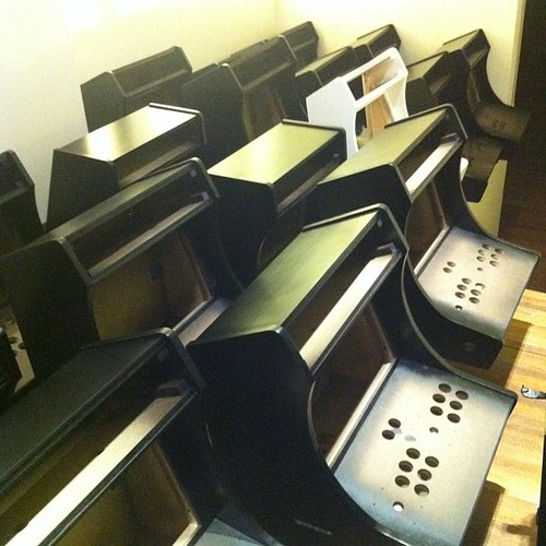
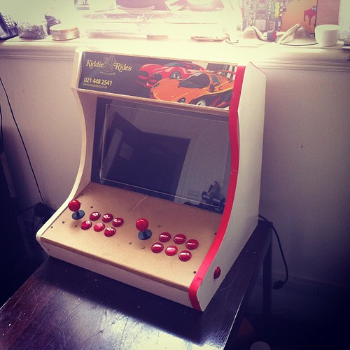
As visitors to my office have noticed, we’ve been building a bunch of arcade machines for clients.
Here are a couple of pics of the builds in progress:
Chassis’s undergoing painting
Unfinished machine
While making those is fun, I also have an interest in what powers them.
Arcade Machines are really just a wooden box, a display, a controller board, input (buttons and joysticks), and a PSU, they’re pretty basic devices. There is an industry cabling standard – JAMMA which makes connecting them up nice and easy.
China has a number of hardware choices for powering them, ranging from PC based boards, original arcade boards, and what I think is the better solution for older games – emulation under embedded ARM/MIPS, vs dedicated boards.
We went through a number of different versions of hardware available here until I found something I liked.
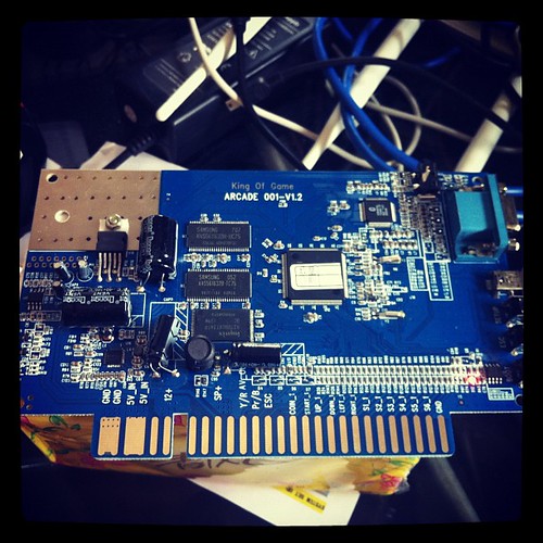
Our currently build hardware du jour runs off of something called “King of Game”.
As is usual in China, no documentation, and the factory is less than forthcoming with information.
Still, not unusual.
The device does have some interesting features for the would be hacker –
It has a nicely labelled “Boot” button, and the component count is quite low. Which generally means its SoC (System on a Chip) based.
The factory has done a little bit of prep work in making sure us ev1l hackorz won’t get at the juicy bits by etching off the cpu.
A quick look at the chip pin count, and the usual choice of chipset SoC more or less got me the right answer in a few minutes though.
My guess was Ingenic 4850, and it turned out to be the Ingenic 4755. This is a MIPS based X-Burst CPU
Even though they’re Chinese vendor, Ingenic does a great job in providing readily available information about their chipset(s). Kudos to the Ingenic guys in Beijing for being so open!
Datasheets for the 4755 and more importantly toolchains are readily available at the Ingenic FTP site – ftp://ftp.ingenic.cn/2soc/4750
Back to the board.
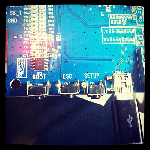
The King of Game board has USB onboard.
Plugging it into a computer shows the flash files available, but unfortunately not the firmware bits I need to see / change (e.g. to upgrade emulator capabilities, and change graphics).
If I hold down boot and plug in the USB, I get prompted for the Ingenic 4750 drivers.
Those are relatively easy to find on the ingenic site, so get a hold of those yourselves.
In order to connect to the board, you use a USB_BOOT.exe (there are also Linux tools available).
I downloaded usbboot-1.4b usbboot1.4b-tools, and unzipped that.
The USB Boot file needs a config file though – and the default config files supplied didn’t work 🙁
So, off to check what could be up.
The USB_Boot utility requires a bunch of settings in order to communicate with a board. After a bit of fiddling playing around with possible options I got it talking to the board.
While I’m not certain I have the settings completely correct here is what I have right now:
[PLL]
EXTCLK 24 ;Define the external crystal in MHz
CPUSPEED 336 ;Define the PLL output frequency
PHMDIV 3 ;Define the frequency divider ratio of PLL=CCLK:PCLK=HCLK=MCLK
BOUDRATE 57600 ;Define the uart boudrate
USEUART 0 ;Use which uart, 0/1 for jz4740,0/1/2/3 for jz4750
[SDRAM]
BUSWIDTH 16 ;The bus width of the SDRAM in bits (16|32)
BANKS 4 ;The bank number (2|4)
ROWADDR 12 ;Row address width in bits (11-13)
COLADDR 9 ;Column address width in bits (8-12)
ISMOBILE 0 ;Define whether SDRAM is mobile SDRAM, this only valid for Jz4750 ,1:yes 0:no
ISBUSSHARE 1 ;Define whether SDRAM bus share with NAND 1:shared 0:unshared
[NAND]
BUSWIDTH 8 ;The width of the NAND flash chip in bits (8|16|32)
ROWCYCLES 3 ;The row address cycles (2|3)
PAGESIZE 2048 ;The page size of the NAND chip in bytes(512|2048|4096)
PAGEPERBLOCK 64 ;The page number per block
FORCEERASE 0 ;The force to erase flag (0|1)
OOBSIZE 64 ;oob size in byte
ECCPOS 6 ;Specify the ECC offset inside the oob data (0-[oobsize-1])
BADBLACKPOS 0 ;Specify the badblock flag offset inside the oob (0-[oobsize-1])
BADBLACKPAGE 127 ;Specify the page number of badblock flag inside a block(0-[PAGEPERBLOCK-1])
PLANENUM 1 ;The planes number of target nand flash
BCHBIT 4 ;Specify the hardware BCH algorithm for 4750 (4|8)
WPPIN 0 ;Specify the write protect pin number
BLOCKPERCHIP 0 ;Specify the block number per chip,0 means ignore
[END]
If I put the board into USB boot mode (hold down boot button, and plug into the usb), then run the USB_TOOL.EXE file I can communicate
 Welcome!

 USB Boot Host Software!

 USB Boot Software current version: 1.4b

 Handling user command.

 USBBoot :> list
Device number can connect :1
USBBoot :> help
Command support in current version:
help print this help;
boot boot device and make it in stage2;
list show current device number can connect;
fconfig set USB Boot config file;
nquery query NAND flash info;
nread read NAND flash data with checking bad block and ECC;
nreadraw read NAND flash data without checking bad block and ECC;
nreadoob read NAND flash oob without checking bad block and ECC;
nerase erase NAND flash;
nprog program NAND flash with data and ECC;
nmark mark a bad block in NAND flash;
go execute program in SDRAM;
version show current USB Boot software version;
exit quit from telnet session;
readnand read data from nand flash and store to SDRAM;
load load file data to SDRAM;
run run command script in file;
memtest do SDRAM test;
gpios let one GPIO to high level;
gpioc let one GPIO to low level;
sdprog program SD card;
sdread read data from SD card;
USBBoot :> boot
Usage: boot (1)
1:device index number
USBBoot :> boot 0
Checking state of No.0 device: Unboot
Now booting No.0 device:
Download stage one program and execute at 0x80002000: Pass
Download stage two program and execute at 0x80c00000: Pass
Boot success!
Now configure No.0 device:
Now checking whether all configure args valid:
Current device information: CPU is Jz4750
Crystal work at 24MHz, the CCLK up to 336MHz and PMH_CLK up to 112MHz
Total SDRAM size is 16 MB, work in 4 bank and 16 bit mode
Nand page size 2048, ECC offset 6, bad block ID 127, use 1 plane mode
Configure success!
Next up, read the firmware off the flash, and dump it to see which version of the Dingoo code they most probably ripped off 🙂
Archives
- November 2024
- November 2019
- October 2019
- August 2019
- April 2019
- February 2017
- September 2016
- June 2016
- May 2016
- September 2015
- August 2015
- June 2015
- April 2015
- December 2014
- October 2014
- September 2014
- July 2014
- June 2014
- April 2014
- October 2013
- July 2013
- May 2013
- April 2013
- March 2013
- January 2013
- December 2012
- October 2012
- August 2012
- July 2012
- June 2012
- May 2012
- April 2012
- March 2012
- December 2011
- November 2011
- October 2011
- September 2011
- July 2011
- May 2011
- April 2011
- March 2011
- February 2011
- January 2011
- December 2010
- November 2010
- October 2010
- September 2010
- August 2010
- July 2010
- June 2010
- May 2010
- April 2010
- March 2010
- February 2010
- January 2010
- December 2009
- November 2009
- October 2009
- May 2009
- April 2009
- March 2009
- February 2009
- January 2009
- December 2008
- November 2008
- October 2008
- September 2008
Categories
- Apple
- Arcade Machines
- Badges
- BMW
- China Related
- Cool Hunting
- Exploits
- Firmware
- Food
- General Talk
- government
- IP Cam
- iPhone
- Lasers
- legislation
- MODx
- MySQL
- notice
- qmail
- requirements
- Reviews
- Service Issues
- Tao Bao
- Technical Mumbo Jumbo
- Things that will get me censored
- Travel
- Uncategorized
- Useful Info