Someone from the JammaForums.co.uk emailed me a copy of the firmware in their SD card from a XinYe 138 in 1.
Card looks something like this:

I don’t have one, but I took a quick look at the data provided, and it looks fairly straightforward to “hack”.
It actually took me less than 30 minutes to have most of the good bits extracted from receiving the file!
There are 2 files on the SD card.
One is a 64 byte file called sn.bin which contains this data:

This looks suspiciously like a header, but I haven’t taken a clear look.
The second file is called x3rodl.bin, and contains a Linux firmware in ARM format.
The first few hundred bytes look like this:

Its obviously in ARM format, as the first set of bytes are ARM no-op codes.
00 00 A0 E1, which repeats 8 times.
02 00 00 EA, then…
18 28 6F 01 – Which is a magic word indicating that this contains a zImage (compressed Linux kernel)
18 28 6F 01 = 0x016f2818
Linux code looks something like this for identifying if its a kernel:
if (*(ulong *)(to + 9*4) != LINUX_ZIMAGE_MAGIC) {

        printk("Warning: this binary is not compressed linux kernel image/n");

        printk("zImage magic = 0x%08lx/n", *(ulong *)(to + 9*4));

    } else {

        printk("zImage magic = 0x%08lx/n", *(ulong *)(to + 9*4));

    }
9 * 4 = 36, which is our location, and this happens to have our magic number.
So, we know its a kernel. Its also probably the VIVI bootloader from Samsung, as that uses that style MAGIC.
The following bits of data, contain the setup for the kernel, and the boot code.
This continues on until the compressed kernel+ramdisk. That starts with 1F 8B 08 (gzip header bytes) over at 0x3EF2, until roughly the end of the file.
I extracted that part and had a quick look.
Its about 7.7M size unpacked.
Linux version is: 2.6.36-FriendlyARM
Boot params are:
console=ttySAC0,115200 root=/dev/ram init=/linuxrc initrd=0x51000000,6M ramdisk_size=6144
RAMDISK File System starts at 0x20000, and looks like this:
lawrence$ ls -al

total 24

drwxr-xr-x  13 lawrence  staff   442 Jun 17 23:09 .

drwxr-xr-x   4 lawrence  staff   136 Jun 17 23:08 ..

drwxr-xr-x  51 lawrence  staff  1734 Jun 17 23:09 bin

drwxr-xr-x   2 lawrence  staff    68 Jun 17 23:09 dev

drwxr-xr-x  11 lawrence  staff   374 Jun 17 23:09 etc

-rwxr-xr-x   1 lawrence  staff  3821 Jun 17 23:09 init

-rw-r--r--   1 lawrence  staff  3821 Jun 17 23:09 init~

lrwxrwxrwx   1 lawrence  staff    11 Jun 17 23:09 linuxrc -> bin/busybox

drwxr-xr-x   2 lawrence  staff    68 Jun 17 23:09 proc

drwxr-xr-x   2 lawrence  staff    68 Jun 17 23:09 r

drwxr-xr-x  19 lawrence  staff   646 Jun 17 23:09 sbin

drwxr-xr-x   2 lawrence  staff    68 Jun 17 23:09 sdcard

drwxr-xr-x   4 lawrence  staff   136 Jun 17 23:09 usr
The bootup script for this looks like this:
#! /bin/sh
PATH=/sbin:/bin:/usr/sbin:/usr/bin
runlevel=S
prevlevel=N
umask 022
export PATH runlevel prevlevel
echo st.
#
# Trap CTRL-C &c only in this shell so we can interrupt subprocesses.
#
trap ":" INT QUIT TSTP
/bin/hostname FriendlyARM
/bin/mount -n -t proc proc /proc
cmdline=`cat /proc/cmdline`
ROOT=none
ROOTFLAGS=
ROOTFSTYPE=
NFSROOT=
IP=
INIT=/sbin/init
#run_fs_image=/images/linux/rootfs_xin1arm_sdhotplug.ext3
for x in $cmdline ; do
case $x in
root=*)
ROOT=${x#root=}
;;
rootfstype=*)
ROOTFSTYPE="-t ${x#rootfstype=}"
;;
rootflags=*)
ROOTFLAGS="-o ${x#rootflags=}"
;;
init=*)
INIT=${x#init=}
;;
nfsroot=*)
NFSROOT=${x#nfsroot=}
;;
ip=*)
IP=${x#ip=}
;;
esac
done
if [ ! -z $NFSROOT ] ; then
echo $NFSROOT | sed s/:/\ /g > /dev/x ; read sip dir < /dev/x
echo $IP | sed s/:/\ /g > /dev/x; read cip sip2 gip netmask hostname device autoconf < /dev/x
rm /dev/x
#echo $sip $dir $cip $sip2 $gip $netmask $hostname $device $autoconf
mount -t nfs $NFSROOT /r -o nolock,proto=tcp
#[ -e /r/dev/console ] || exec /bin/sh
elif [ ! -z $run_fs_image ] ; then
#lilxc
#echo $run_fs_image
echo sdroot.
if [ ! -e /dev/mmcblk0p2 ] ; then
echo "p2 not found."
reboot
sleep 5
fi
ROOTFSTYPE="-t ext3"
for i in 1 2 3 4 5 ; do
#/bin/mount -n -o sync -o noatime -o nodiratime -o ro -t vfat /dev/mmcblk0p1 /sdcard && break
/bin/mount -n -o sync -o noatime -o nodiratime -o ro -t ext3 /dev/mmcblk0p2 /sdcard && break
echo Waiting for SD Card...
if [ $i = 4 ] ; then
echo " p2 failed. "
reboot
sleep 5
break;
fi
sleep 1
done
#echo ------begin----------------------------------------
#sleep 1
#lilxc
#ls -l /dev
#sleep 1
#echo -----------------------------------------------
#ls -l /sdcard
#sleep 1
#echo ------end------------------------------------------
#/sbin/losetup /dev/loop0 /sdcard/$run_fs_image
#/bin/mount $ROOTFSTYPE /dev/loop0 /r
#/bin/mount $ROOTFSTYPE -o noatime -o nodiratime -o ro /dev/mmcblk0p2 /r > /dev/null 2>&1
/bin/mount $ROOTFSTYPE -n -o noatime -o nodiratime -o ro /dev/mmcblk0p3 /r > /dev/null 2>&1
mount -o move /sdcard /r/sdcard
#/sbin/losetup /dev/loop1 /r/sdcard/swap
#/sbin/swapon /dev/loop1
else
# /bin/mount -n $ROOTFLAGS $ROOTFSTYPE $ROOT /r
# echo "Readonly mount...(lilxc)"
# mount -n -t yaffs2 -o noatime -o nodiratime -o ro /dev/mtdblock2 /r
# mount -n -t yaffs2 -o noatime -o nodiratime /dev/mtdblock2 /r
mount -n -t yaffs2 -o noatime -o nodiratime -o ro /dev/mtdblock2 /r
if [ -e /r/home/plg/reboot ]; then
umount /r
mount -n -t yaffs2 -o noatime -o nodiratime /dev/mtdblock2 /r
fi
fi
ONE_WIRE_PROC=/proc/driver/one-wire-info
ETC_BASE=/r/etc
[ -d /r/system/etc ] && ETC_BASE=/r/system/etc
[ -e $ETC_BASE/ts.detected ] && . $ETC_BASE/ts.detected
[ -z $CHECK_1WIRE ] && CHECK_1WIRE=Y
if [ $CHECK_1WIRE = "Y" -a -e $ONE_WIRE_PROC ] ; then
if read lcd_type fw_ver tail < $ONE_WIRE_PROC ; then
if [ x$lcd_type = "x0" -a x$fw_ver = "x0" ] ; then
TS_DEV=/dev/touchscreen
else
TS_DEV=/dev/touchscreen-1wire
echo "1Wire touchscreen OK"
fi
if [ -e $ETC_BASE/friendlyarm-ts-input.conf ]; then
sed "s:^\(TSLIB_TSDEVICE=\).*:\1$TS_DEV:g" $ETC_BASE/friendlyarm-ts-input.conf > $ETC_BASE/ts-autodetect.conf
mv $ETC_BASE/ts-autodetect.conf $ETC_BASE/friendlyarm-ts-input.conf -f
echo "CHECK_1WIRE=N" > $ETC_BASE/ts.detected
fi
fi
fi
[ -e /r/etc/friendlyarm-ts-input.conf ] && . /r/etc/friendlyarm-ts-input.conf
[ -e /r/system/etc/friendlyarm-ts-input.conf ] && . /r/system/etc/friendlyarm-ts-input.conf
export TSLIB_TSDEVICE
#lilxc debug here
#/bin/mount -n -o sync -o noatime -o nodiratime -t vfat /dev/mmcblk0p1 /sdcard
#cp /sdcard/lktcmd /r/tmp
#exec /bin/sh
# for running game
umount /proc
exec switch_root /r $INIT /r/dev/console 2>&1
The secondary loader in init looks like this:
#! /bin/sh
PATH=/sbin:/bin:/usr/sbin:/usr/bin:/usr/local/bin:
runlevel=S
prevlevel=N
umask 022
export PATH runlevel prevlevel
#
# Trap CTRL-C &c only in this shell so we can interrupt subprocesses.
#
trap ":" INT QUIT TSTP
/bin/hostname FriendlyARM
[ -e /proc/1 ] || /bin/mount -n -t proc none /proc
[ -e /sys/class ] || /bin/mount -n -t sysfs none /sys
[ -e /dev/tty ] || /bin/mount -t ramfs none /dev
/bin/mount -n -t usbfs none /proc/bus/usb
echo /sbin/mdev > /proc/sys/kernel/hotplug
/sbin/mdev -s
/bin/hotplug
# mounting file system specified in /etc/fstab
mkdir -p /dev/pts
mkdir -p /dev/shm
/bin/mount -n -t devpts none /dev/pts -o mode=0622
/bin/mount -n -t tmpfs tmpfs /dev/shm
/bin/mount -n -t ramfs none /tmp
/bin/mount -n -t ramfs none /var
mkdir -p /var/empty
mkdir -p /var/log
mkdir -p /var/lock
mkdir -p /var/run
mkdir -p /var/tmp
/sbin/hwclock -s
echo " " > /dev/tty1
echo "System starting... " > /dev/tty1
syslogd
#/etc/rc.d/init.d/netd start
#echo " " > /dev/tty1
#echo "Starting networking..." > /dev/tty1
#sleep 1
#/etc/rc.d/init.d/httpd start
#echo " " > /dev/tty1
#echo "Starting web server..." > /dev/tty1
#sleep 1
#/etc/rc.d/init.d/leds start
#echo " " > /dev/tty1
#echo "Starting leds service..." > /dev/tty1
#echo " "
#sleep 1
/etc/rc.d/init.d/mkjoy
#echo " " > /dev/tty1
#echo "System Starting... " > /dev/tty1
#echo " " > /dev/tty1
#echo " " > /dev/tty1
/etc/rc.d/init.d/alsaconf start
#echo "Loading sound card config..." > /dev/tty1
#echo " "
#/sbin/ifconfig lo 127.0.0.1
#/etc/init.d/ifconfig-eth0
#/bin/qtopia &
#echo " " > /dev/tty1
#echo "Starting Qtopia, please waiting..." > /dev/tty1
cd /sdcard
./run.sh
reboot
Fairly easy to reverse!
Refs:
http://www.jammaplus.co.uk/
http://blog.csdn.net/liangkaiming/article/details/6259189
As I’ve been reasonably successful in the past at figuring out file systems from flat files, I thought I’d have a go at the Dell Mini 3i 1.5 Firmware that surfaced at damipan (http://www.namipan.com/d/DELL_MINI3I_OMS1.5.rar/a5ba3b06ab0bfc9baeb2f09b44f54aa40bac3457ee8ebc04)
The rar file unzips to a MFF file.
This I’m probably guessing is probably named after Marvell File Format or Marvell Flasher File.
Here’s my initial work on the file system of MFF format, based on DELL_Mini3i_OMS1.5.mff
Initial 80 bytes [0x0 – 0x080] (MFF HEADER)
0x00 – 0x03 : 3 Bytes Header MFF
0x03 – 0x07 : Still to figure out, probably file length or crc.
Have to grab another firmware file to check though..
0x08 : Number of files? 9 listed, so quite probably…
Rest of header padded out with zero’s to end of 80 bytes.
[0x80 – 0x180] File Allocation Table
0x80 – our first file. Looks like 0x100 / 256 bytes per file listed, padded with 0x0’s
File listing looks like this:
File header (for each file)
8 bytes, then filename, padded with 0’s to fill 256 bytes length
First 4 bytes – offset in MFF of start of file.
Second 4 bytes – length of file.
Remaining files repeat from next 256 byte intervals.
eg
0x180 – 0x280
0x280 – 0x380
…
[0x80 + 9 files x 0x100 bytes = 0x980] Start of Data.
How did I work this out?
HEADER | Filename (not in hex below as easier to read)
80 09 00 00 34 BB 00 00 | Tavor Flasher_Samsung_ONENAND_h.bin
0x0980 is the start of our first file data, so the first 2 bytes are definitely File Start.
0xBB34 looks quite possibly like File Length.
We can check this easily with one of the plain text files.
Flash_Protection_table.ini is prefixed with 63 EA AD 09 4B 00 00 00
So it should start at 0x09 AD – hmm, readable text starts at offset 9AD D564.
Not quite right. Start offset looks close though.
Lets look at another one.
Tavor_saar_onenand.ini – prefix says
64 d5 ad 09 6f 01 00 00
Ah, 0x9 AD D5 64 is actually our Tavor_saar_onenand.ini content. Cool, a match. So, the first 4 bytes are definitely our location pointer.
Lets look at the Flash protection table again Flash_Protection_table.ini
63 EA AD 09 | 4B 00 00 00
Should start at 09 AD EA 63, and go for 4B length. Bingo, it does 🙂
Our file contents for that area are:
[PROTECTED_REGION_0]
Block_Offset=0x100000
Length=0x20000
Mode=SKIP_BLOCKS
So, now we can start to split the files apart into their associated parts.
factory_BENZ2GWIFI.fbf is probably going to be the most interesting, as its the largest.
That starts at 0xC564, length of 0x09AD1000 and starts with “Marvell_FBF”
Basic math says that 0x9ADD564 (0x09AD1000 + 0xC564) should be our end of file.
Well, it is, as we know flash protection table.ini starts at 9add564.
So, should be fairly easy with that info to write an unpacker tool to rip out the first interior files from the MFF file format.
Some of the files inside are also “packed”, but those appear to be fairly easy to rip apart also 🙂
I’m guessing with a bit more work I’ll be able to replace parts of the firmware with different versions quite soonish.
The file I’m using off of namipan has the following files inside:
TavorFlasher_SAMSUNG_ONENAND_h.bin
TavorFlasher_SAMSUNG_ONENAND_TIM.bin
factory_BENZ2GWIFI.fbf
Tavor_SAAR_OneNAND.ini
factory_BENZ2GWIFI.mff.mlt
magic_fbf.ini
magic_fbf_inner.ini
NTIM_fbw.ini
Flash_Protection_Table.ini
I’m guessing that our fbf file will probably be able to be split into parts as per our ntim_fbw.ini data.
FBF = Flash Binary Format?
some interesting files listed
ntim.bin – non trusted image module?
blob_full.bin – from the borq’s blob gz?
Tavor_M05_Poleg_AI_B0_Flash.bin – tavor = our product chip, as we’re running on a Marvel PXA935 (aka Tavor-P65)
Interesting thing of note – our OEM UniqueID: 0xF00F00 in Unicode is what glyph?
Hint – its not an orange, or a pear 😉
NTIM_fbw.ini
Version: 0x030102
Trusted: 0Issue Date: 0x08142006
OEM UniqueID: 0xf00f00
Boot Flash Signature: 0x4e414e02
Number of Images: 10
Size of Reserved in bytes: 0x40Image ID: 0x54494D48
Next Image ID: 0x4F424D49
Flash Entry Address: 0x0
Load Address: 0x5c008000
Image Size To CRC in bytes: 0x0
Image Filename: NTIM.binImage ID: 0x4F424D49
Next Image ID: 0x4F534C4F
Flash Entry Address: 0x20000
Load Address: 0x5c013000
Image Size To CRC in bytes: 0x0
Image Filename: obm_full.binImage ID: 0x4F534C4F
Next Image ID: 0x5349474E
Flash Entry Address: 0x80000
Load Address: 0x83000000
Image Size To CRC in bytes: 0x0
Image Filename: blob_full.binImage ID: 0x5349474E
Next Image ID: 0x494D4549
Flash Entry Address: 0x00120000
Load Address: 0x84000000
Image Size To CRC in bytes: 0x0
Image Filename: signature_full.binImage ID: 0x494D4549
Next Image ID: 0x4152424C
Flash Entry Address: 0x00100000
Load Address: 0xBFEE0000
Image Size To CRC in bytes: 0x0
Image Filename: reliable_full.binImage ID: 0x4152424C
Next Image ID: 0x47524249
Flash Entry Address: 0x00140000
Load Address: 0xBF600000
Image Size To CRC in bytes: 0x0
Image Filename: arbel_full.binImage ID: 0x47524249
Next Image ID: 0x62746C67
Flash Entry Address: 0x00840000
Load Address: 0xBFF00000
Image Size To CRC in bytes: 0x0
Image Filename: tavor_full.binImage ID: 0x62746C67
Next Image ID: 0x70636C67
Flash Entry Address: 0x00A00000
Load Address: 0xBF300000
Image Size To CRC in bytes: 0x0
Image Filename: bootlogo_full.binImage ID: 0x70636C67
Next Image ID: 0x464F5441
Flash Entry Address: 0x00A20000
Load Address: 0x8F300000
Image Size To CRC in bytes: 0x0
Image Filename: prechangelogo_full.binImage ID: 0x464F5441
Next Image ID: 0xFFFFFFFF
Flash Entry Address: 0x0EA40000
Load Address: 0x80100000
Image Size To CRC in bytes: 0x0
Image Filename: fota_full.binReserved Data:
0x4F505448
0x00000002
0x55415254
0x00000010
0x00004646
0x00000001
0x50524F49
0x00000020
0x00000002
0x00000000
0x00000000
0x00000000
0x00000001
0x00000000
0x5465726D
0x00000008
Flash_Protection_Table.ini
[PROTECTED_REGION_0]
Block_Offset=0x100000
Length=0x20000
Mode=SKIP_BLOCKS
magic_fbf_inner.ini
[INTEL_FLASH_DEVICE_INPUT_FILE]
Number_of_Images=20[IMAGE_HEADER_0]
Start_Address=0xfa00000
Image_Length=0x80000
EraseBlocks=1
WriteImage=0
VerifyWrite=0[IMAGE_HEADER_1]
Start_Address=0xdd40000
Image_Length=0x800000
EraseBlocks=1
WriteImage=0
VerifyWrite=0[IMAGE_HEADER_2]
Start_Address=0xeb40000
Image_Length=0x8c0000
EraseBlocks=1
WriteImage=0
VerifyWrite=0[IMAGE_HEADER_3]
Filename=NTIM.bin
Start_Address=0x00000000
EraseBlocks=1
WriteImage=1
VerifyWrite=0[IMAGE_HEADER_4]
Filename=Arbel_NVM_SAC_NOCOMMRTC.bin
Start_Address=0x00140000
EraseBlocks=1
WriteImage=1
VerifyWrite=0[IMAGE_HEADER_5]
Filename=blob
Start_Address=0x00080000
EraseBlocks=1
WriteImage=1
VerifyWrite=0[IMAGE_HEADER_6]
Start_Address=0x0bd40000
Image_Length=0x02000000
EraseBlocks=1
WriteImage=0
VerifyWrite=0
[IMAGE_HEADER_7]
Filename=opl.img.yaffs
Start_Address=0x0bd40000
EraseBlocks=1
WriteImage=1
VerifyWrite=0[IMAGE_HEADER_8]
Filename=ramdisk_len.img
Start_Address=0x00c40000
EraseBlocks=1
WriteImage=1
VerifyWrite=0[IMAGE_HEADER_9]
Filename=ramdisk-recovery_len.img
Start_Address=0x00cc0000
EraseBlocks=1
WriteImage=1
VerifyWrite=0[IMAGE_HEADER_10]
Start_Address=0x00d40000
Image_Length=0x08000000
EraseBlocks=1
WriteImage=0
VerifyWrite=0
[IMAGE_HEADER_11]
Filename=system.img.yaffs
Start_Address=0x00d40000
EraseBlocks=1
WriteImage=1
VerifyWrite=0[IMAGE_HEADER_12]
Filename=TAVOR_LINUX_NTOBM.bin
Start_Address=0x00020000
EraseBlocks=1
WriteImage=1
VerifyWrite=0[IMAGE_HEADER_13]
Filename=Tavor_M05_Poleg_AI_B0_Flash.bin
Start_Address=0x00840000
EraseBlocks=1
WriteImage=1
VerifyWrite=0[IMAGE_HEADER_14]
Start_Address=0x08d40000
Image_Length=0x03000000
EraseBlocks=1
WriteImage=0
VerifyWrite=0
[IMAGE_HEADER_15]
Filename=userdata.img.yaffs
Start_Address=0x08d40000
EraseBlocks=1
WriteImage=1
VerifyWrite=0[IMAGE_HEADER_16]
Filename=zImage
Start_Address=0x00a40000
EraseBlocks=1
WriteImage=1
VerifyWrite=0[IMAGE_HEADER_17]
Filename=prdcfg.bin
Start_Address=0x00940000
EraseBlocks=1
WriteImage=1
VerifyWrite=0[IMAGE_HEADER_18]
Filename=precharge_logo.out
Start_Address=0x00a20000
EraseBlocks=1
WriteImage=1
VerifyWrite=0[IMAGE_HEADER_19]
Filename=logo_pic.gz.out
Start_Address=0x00a00000
EraseBlocks=1
WriteImage=1
VerifyWrite=0
Lastly, hi to the people at http://www.allphone.com.cn 😉
As I’ve been busy with real life ™, its been a while since I took a trip to the computer mall to see what new goodies I could play with.
A friend is in town from Beijing, so took him down to the Shanzhai hell (or heaven depending on PoV) that is Qiu Jiang lu.
I wasn’t aware that you could buy Keychain video recorders for 80rmb, but you can. Apparently they’re even cheaper in eBay – although I don’t see how its possible, given that the factories here are pricing higher than they sell for in the States. Rejects?
Anyhow, I bought 2 keychain video camera’s, and an MP3 looking one.

Dissected one and it contains the Anyka AK3651B as the main chip.
The AK36xx series is an SoC (System on a Chip).

As Anyka appears to be deathly afraid of giving out any useful information about their products, I’ve had to piece together info from what I found online.
Their own product page here – http://www.anyka.com/enProShow.asp?sortFlag=110&sortName=Application%20Processor&id=105
says the following:
32-bit Microprocessor Core
Integrated I/D cache
Memory Management Unit (MMU)Video Coprocessor
MPEG4.SP codec
H.263 codec
Motion JPEG codecAudio Coprocessor
MP3 decoder
WMA decoder
AAC/AAC+ decoder
AMR codec
Real-time audio stream in PCM/ADPCM formatImage Coprocessor
JPEG HW codecGlueless Dual LCD Displays
Supporting MPU LCD
Supporting RGB LCD
Programmable LCD size and refreshing rateConnectivity
USB 2.0 HS OTG
I2S master/slave
UART
SPI
MMC/SDEmbedded ADCs and DACs
SAR ADC for touch panel and voltage detect
Sigma-Delta ADC for microphone
Sigma-Delta DACs for stereoBuilt-in Power Amplifier/Headphone Driver
External Memory Support
Supporting SDRAM
Supporting Nand Flash (SLC/MLC, with hardware ECC)Package
LQFP 128-pin/144-pin,FBGA 100-pin/144-pin
Appears that they’re mostly used in MP3/MP4 players, which is why most of my googling on specs was ruined by whiny users asking for someone to please help them with their foobar’d player.
The first useful links on these are at Chuck’s pages here – http://www.chucklohr.com/808/
He’s done a lot of useful work collating information, although some of his deductions are a little strange, so take some things with a pinch of salt. Lots of good info though.
The main source of info on the hardware side is at http://www.readerme.com, they have a most excellent section of downloads which provide more information on the chips than anything else out there!
We gave them a call and had a chat (one of the benefits of being located in China, is that we obviously speak Chinese in the office!).
They don’t speak great Mandarin though – so it was bad cantonesedarin or Mandonese? Hmm, have to come up with a word for that! (similar to Chinglish but mixing Cantonese and Mandarin).
Both sides were laughing but we could at least talk to each other. “Mo man tai, dui ma?”
They actually don’t sell products, they only do design work for others, but, thats good to know.
They did point us in the direction of a few trading companies that could do FOB export, but shipping quantities are in the x,000’s so not so useful yet.
I’ll see if I can find the actual factories making these tomorrow. (Although when I say we, I mean the staff).
They did prove to be an excellent source of data on the chips though if one takes a look at the PDF’s on their site.
The golden data trove is here – http://www.readerme.com/html/html/%E7%9B%B8%E5%85%B3%E4%BA%A7%E5%93%81%E5%8E%9F%E7%90%86%E5%9B%BE%EF%BC%8C%E8%B4%B4%E7%89%87%E5%9B%BE.html
According to Anyka (安凯 in Chinese) the 36xx chips are a series, so they should have similar functionality.
While I don’t have data sheets, or a BSP, I can read the PDF’s at least to get an idea of where things are laid out.
AK3631B

AK3651B

They do look similar, so probably only minor differences in functionality (probably the newer ones are cheaper?).
Again, hard to check, as Anyka datasheets appear to be hens teeth.
I may give them a call also, and see if they’ll be willing to give us some info about their products, but I’m not holding my breath on that one.
I’ve also poked around a bit in the firmware files using strings, and taking a look at headers, and have come up with some preliminary conclusions.
I’m guessing their SoC is ARM5 based, given what i have found (haven’t decompiled yet, but looks like that).
Some common strings in the firmware’s from start:
00000 06 00 00 EA FE FF FF EA
Googling “06 00 00 EA FE FF FF EA” comes up with some other people talking about firmware for pxa312 devices, which have exactly that in their boot loader, so, seems likely.
The PXA312 is ARMv5TE…
I’m guessing some playing around with radare (http://radare.nopcode.org/get/radare.pdf.html) should get some more info about whats going on.
Running strings on the firmware files available shows interesting info:
strings /Documents/Keychain\ Camera/cx311V2.04/Spiboot_36XX.bin
ANYKA362
6KA49
start read cfg
file cnt:%d
file name:%s
Cannot find BIOS
read file info fail
load bios ……
map:%d
file len:%d
ld addr:0x%x
Load bios from spiflash successfuly!
read BIOS fail
spi boot start
system clock: %d
BIOS
Thats our 4k bootloader, which obviously loads our 1M bios image from SPI flash memory (SPI = Serial Peripheral Interface)
More on SPI here.
http://en.wikipedia.org/wiki/Serial_Peripheral_Interface_Bus
Hmm, more reasons for me to get a Bus Pirate now…
We have a flasher also, although its Windows based.
I’m guessing some USB sniffing will lead to some magic byte handshake sequence to get into the bootloader via USB, as the BIOS strings point to that.
eg:
“The setup packet is not 8 byte!”
Also amusing is that its fairly easy to find the FAT32 code embedded in at least one of the firmwares
EB xx 90 … -> 55 AA (in Sprint1M.bin)

The flasher tool is also nice enough to give us an idea of layout in the 1M flash chip.
You’ll need to install the Anyka M3 USB driver to talk to the chip, which appears to have the following attributes via USB:
Vendor ID: 0471
Product ID: 0666 (the product of the beast? hehe)
This is a bit naughty, as 0471 is in theory already taken by Philips (or NXP) according to http://www.linux-usb.org/usb.ids
Its also astoundingly obvious that they used driverworks to make the driver. (From the oh so copied in China vid/pid, and the strings left in the driver). An example of this here http://www.baiheee.com/OpenSource/Easy%20USB%2051%20Programer/Easy%20USB%2051%20Programer_DriveOurBoard.htm
Want to bet someone read those instructions and its been repeated ad nauseum?
Sadly, its so easy to see the minimal effort that’s gone into things.
Back to our flasher, it says that our 1M chip is laid out as follows:
###Project Name
project name = chaoxian###Devie Number
device channel = 8###COM
com bOpen = 0
com base = 1
com count = 1
com baud rate = 38400path producer sundance2 = producer_sundance2.bin
path producer sundance2A uboot = producer_sundance2A_uboot.bin
path producer sundance2A umass = producer_sundance2A_umass.bin
path nandboot sundance2= Spiboot_36XX.bin
path nandboot sundance2A= Spiboot_36XX.binbios run addr = 0x30500000
bios start addr = 0xc0000
bios end addr = 0x1c0000
bios backup start addr = 0x1c0000
bios backup end addr = 0x2c0000chip type = AK_3225
chip uboot = 1
chip power off gpio = 255
chip usb2 = 0
chip get aid = 0
chip update = 0
chip select loop = 1
chip select nand0 = 1
chip select nand1 = 1
chip select nand2 = 1
chip select nand3 = 1
chip gpio_ce2 = 255
chip gpio_ce3 = 255ram size = 8
ram row = 12
ram column = 8
ram bank = 4moduleburn DownloadMode = 2
moduleburn bDownloadFLS = 1
moduleburn bDownloadEEP = 1
moduleburn baudrate = 921600
moduleburn gpio_dtr = 85
moduleburn gpio_module_igt = 109
moduleburn gpio_module_reset = 87
moduleburn path_fls = LCG2.fls
moduleburn path_eep = LCG2.eepfs start addr = 0x6c0000
fs reserver block = 64
fs nonfs reserve size = 4partition count = 0
download_to_udisk count = 0
download_to_nand count = 3
download_to_nand1 = 0, Spring1M_bios.bin, 0x30500000, BIOS
download_to_nand2 = 0, Spring.bin, 0x30000000, MMI
download_to_nand3 = 0, AkResData.Bin, 0x0, RESdownload_to_mtd count = 0
nand supported count = 0
If we take a look at that, our Spring1M_bios.bin starts off at C000
(bios start addr = 0xc0000)
(Deduct a 0 as we’re not offset by 0x300000000)
A look in a hex editor at that position shows:

Note the 32bit word value – 0xE1A0C00D
Thats classic ARM, so we _know_ its arm based…
romStart [0xe1a0c00d] mov r12,r13
Our next line of code is exactly the same as listed here http://code.google.com/p/milestone-overclock/wiki/Disassembly
e1a0c00d mov ip, sp
e92dd8f0 push {r4, r5, r6, r7, fp, ip, lr, pc}
So its looking like we can basically disassemble the code using arm-none-linux-gnueabi-objdump
I’ll leave that for another day, but with a bit more work we could compile our own code for this as we now have a good idea of the target cpu.
The next step would be to get into the bootloader or debug mode via USB, and see what can be seen.
Tools used:
0xED – http://www.suavetech.com/0xed/0xed.html
A nice fast and compact hex viewer for OSX.
strings – built into most *nix based systems.
Grey matter – Available to all, unused by many 😉
Now hopefully I can get back to the Webcam firmware stuff as I’ve been promising to do.
I have a couple of older Mac Pro desktops that I tend to.
As my machines usually get upgraded to the max, they’re still pretty darn useful.
Currently they’re all Dual Quad Core 3Ghz / 16G Ram 1,1->2,1 flashed, which is more than enough for dev purposes.
Sadly though, they still have the original graphics cards – rather crappy 7300GT’s.
One of the issues with the Mac Pro 1,1 is that in Yosemite* the original graphics cards aren’t really supported.
*Sure Yosemite isn’t really supported either, but it does work after a bit of EFI boot mangling.
You can work around things, by having a newer NVidia card (i.e. anything 6XX and above), but then you lose boot graphics till the OS loads drivers.
As I sort of quite need boot graphics due to the bootloader side of things getting borked on occasion, I thought I’d source myself a compatible card.
There aren’t really that many options unfortunately for vintage equipment, its mostly 8800GT’s that are at least 5 years+, and priced at silly money.
There are other options though – certain PC graphics cards are usable.
As a Mac Pro 1,1 (2,1), it needs a card that:
#1 – Shipped on a Mac Pro 1,1 or 2,1 (so that AMD created an _EBC_ based Mac BIOS).
#2 – Has a flashable BIOS. This rules out most of the NVidia’s of that era, so its a select number of ATI cards.
Netkas.org is a good source of reading for that sort of thing.
ATI 4870 appears to be flashable, and wasn’t too “$$ bills yo!” on Taobao
So, sourced myself a 4870 1G card (235RMB w/shipping), and set to work.
There is a wealth of information out there about flashing, but unfortunately all the links appear to be pretty dead.
The general consensus is to dump the original firmware, then patch it yourself. There are tools for this, but they don’t really work. Cindori’s Zeus et al..
I tried to do this inside the Mac Pro itself, but it wasn’t having any of it, and didn’t like the perfectly fine DOS USB key(s) I made. Luckily I also had a Windows box available to dump / flash.
Fun and games with PSU connectors later, I booted off a DOS boot disk, used ATIFlash to dump my original rom, then shutdown again.
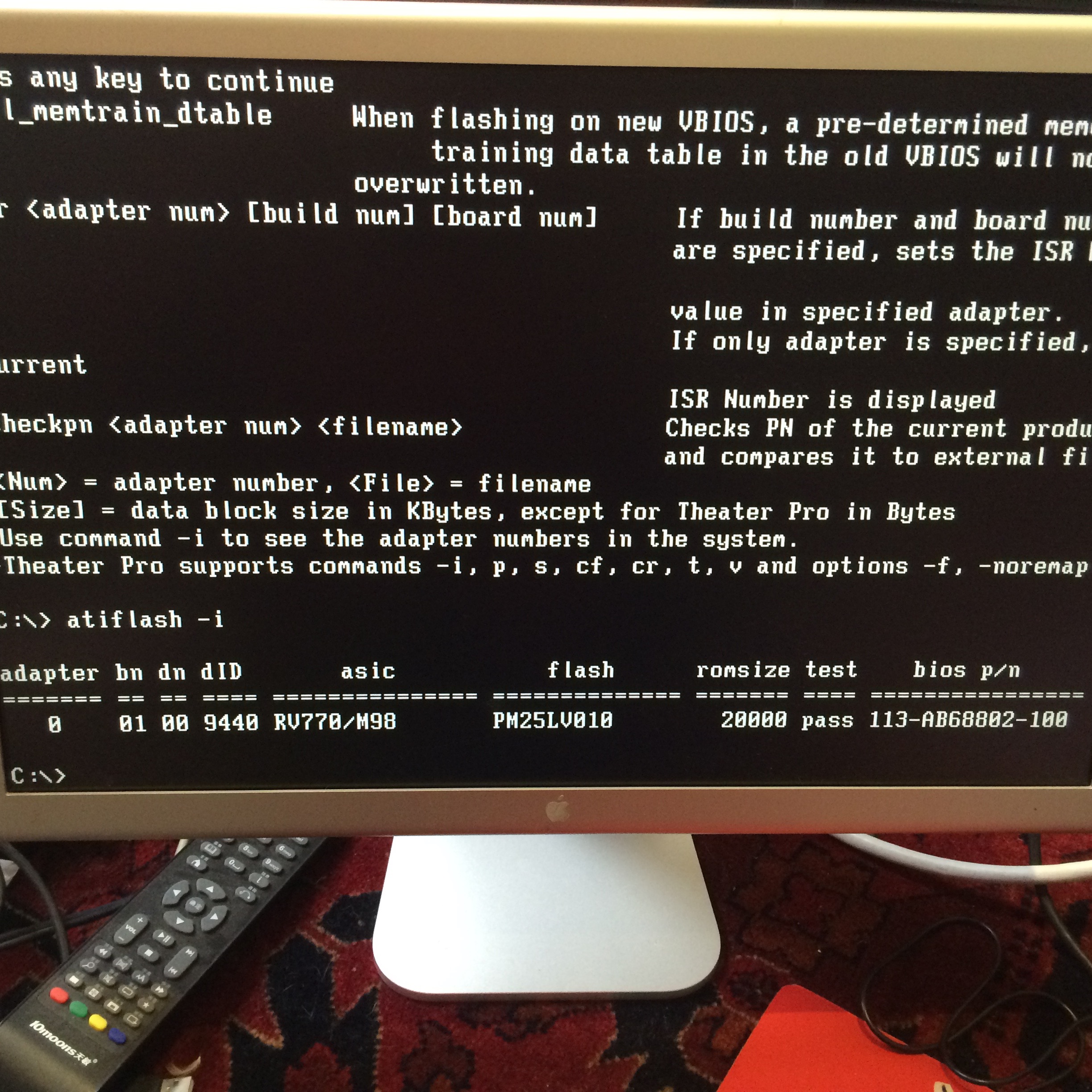
Stuck the USB key back in my laptop, used a ROM I found inside Zeus (show package contents, copy the 4870EFI.ROM out) + patch that with my dumped rom using fixrom.py from here – http://forum.netkas.org/index.php/topic,692.0.html and the patch instructions here – http://forums.macrumors.com/threads/race-to-dump-the-4870-rom-whos-first.661681/page-14#post-7297669
Copied the patched rom back onto the USB, rebooted off again into the DOS boot disk on my Window box, and flashed the new patched EBC rom bios.
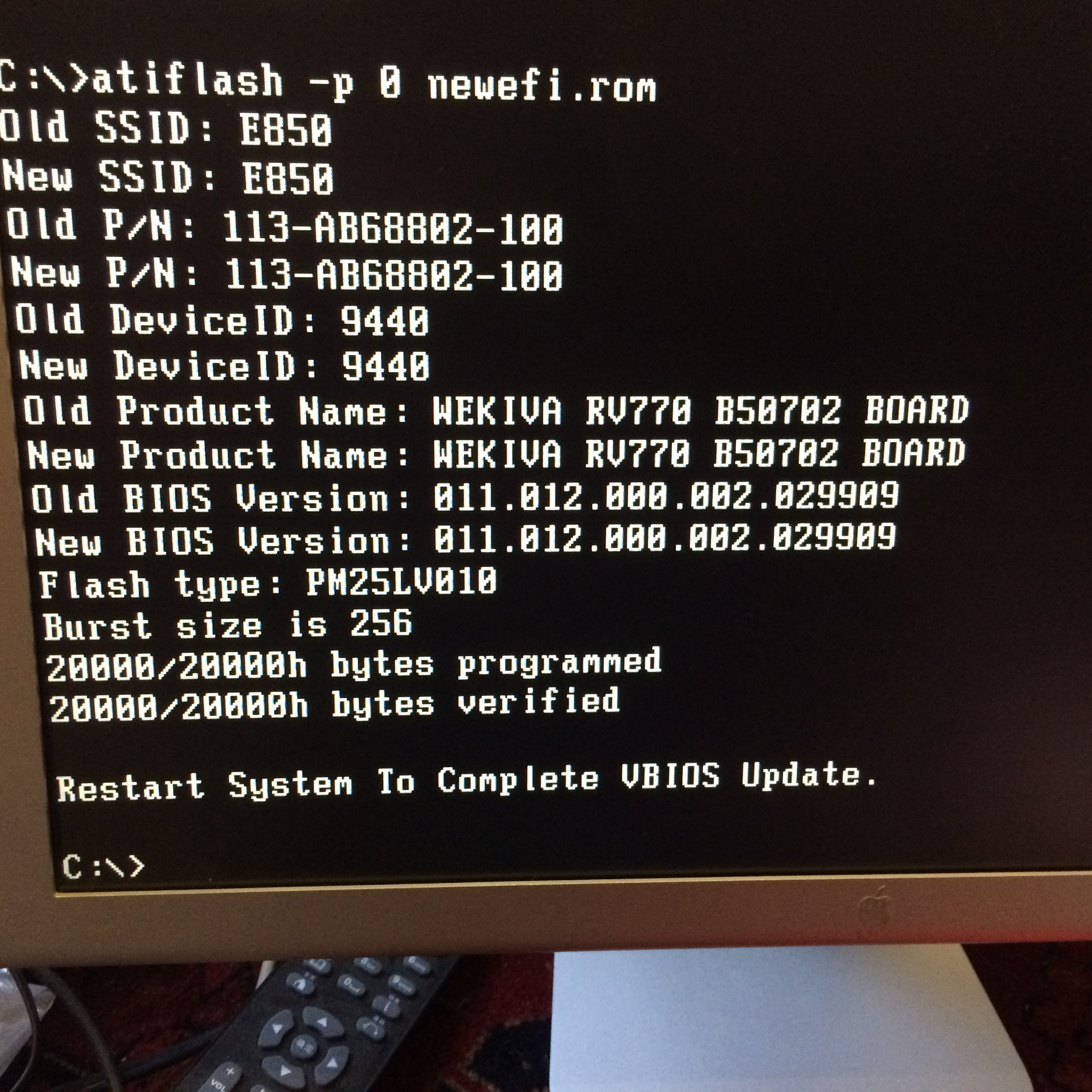
A few minutes of recabling later on the Mac, I got a nice boot screen off the card.
Works fine in OSX too (sleep etc appear to be fine).
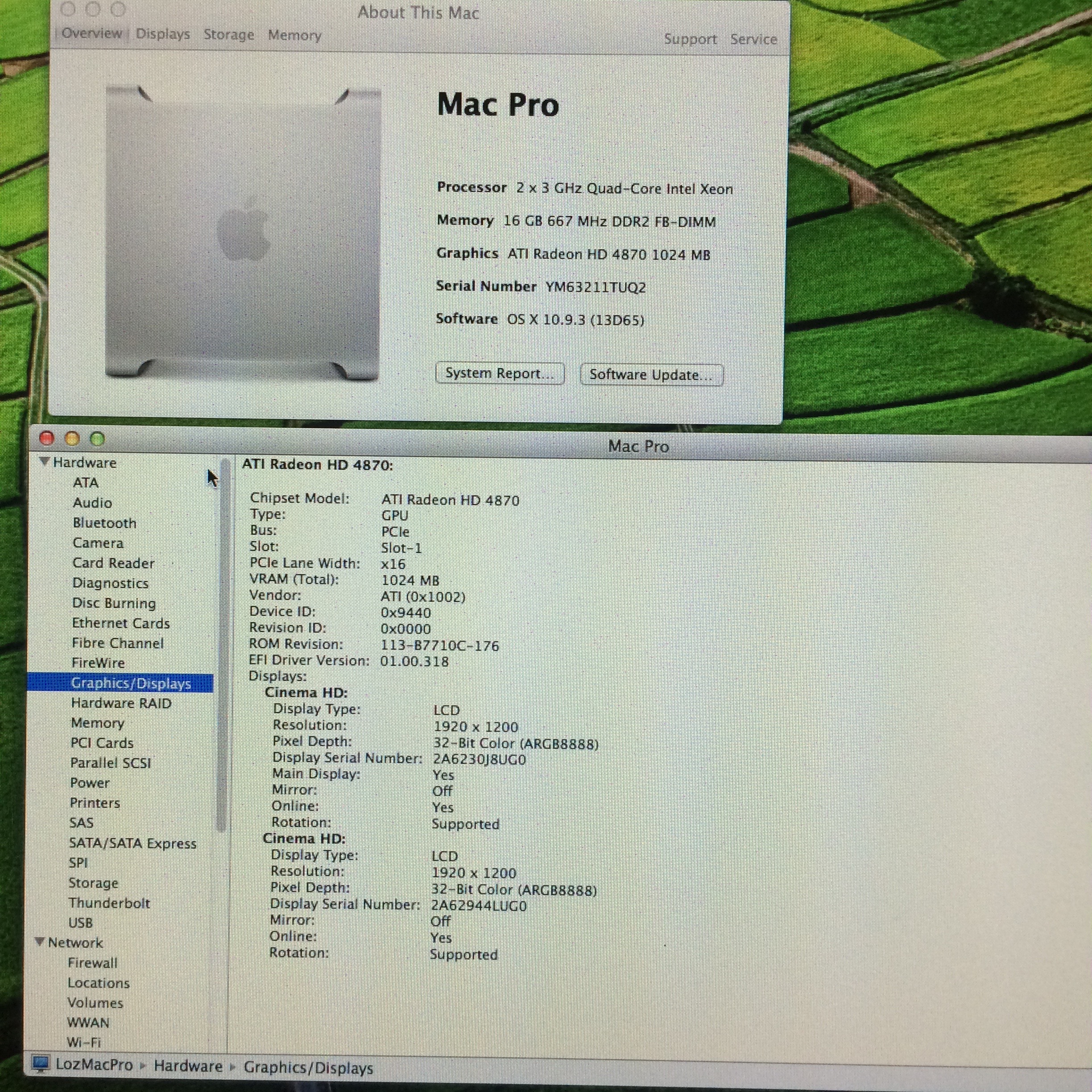
As this was a royal pain in the ass, I have the pre-patched rom here – ROM
Its specifically for the 4870 card I have, so don’t randomly flash to your 4870 card, unless the part number matches. My P/N is below.
Radeon HD4870 1G Dual DVI
PN 288-20E85-230AC
Enjoy.
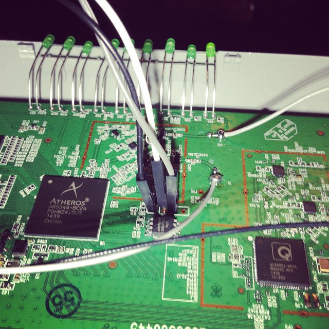
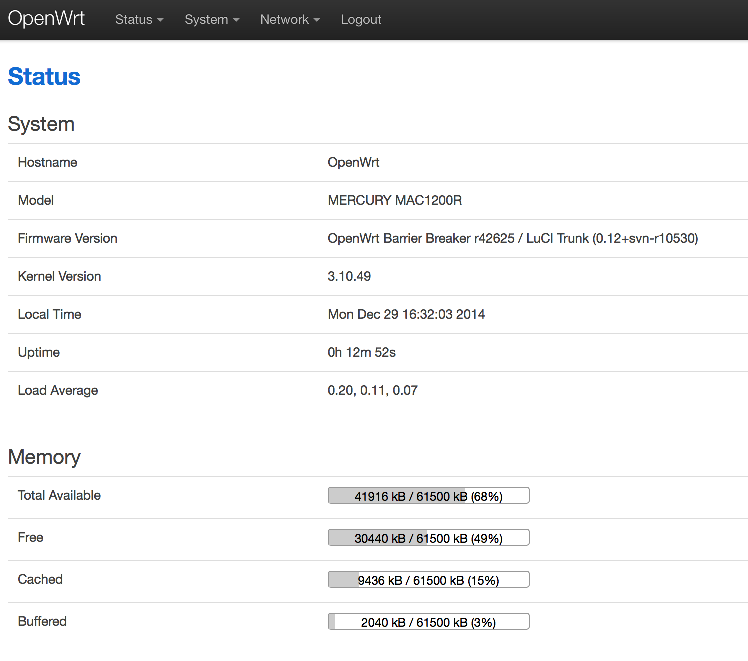
The Mercury MAC1200R (TPLINK WR6300) is one of the cheapest AC based routers on the planet, as I have a few AC devices I thought I’d buy one to try out. They’re available for under RMB120 or so online.
Mercury hardware is TPLink hardware, albeit using a different name. Same stuff, same factory, different casing.
The router has 64M ram, and 8M flash. CPU / Wifi AR9344 / QCA9882
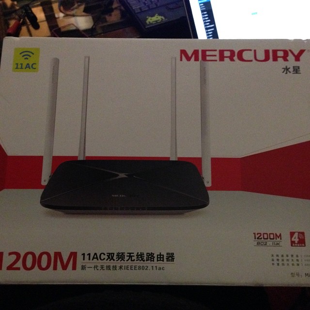
OpenWRT says it has support, so I had a quick go at taking a look at flashing one.
First steps:
Open up the unit (remove the 2 screws underneath, then use a spare credit card or similar to jam open the plastic case).
The serial headers are to the right of the SoC.
You’ll need a rs232 to ttl or usb to ttl adaptor.
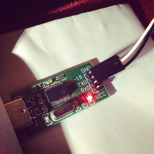
Pin 1 is GND
Pin 2 is TX (connect to rx)
Pin 3 is RX (connect to tx)
Pin 4 is VCC (don’t connect).
Port speeds are 115200,8,n,1
Connect up, and you should see a flurry of activity on boot.
To get into the bootloader (uBoot), you’ll need to type tpl
May take a few tries, so prepare to pull power and retry again, and again till you get in.
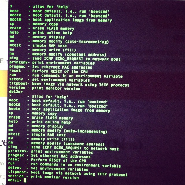
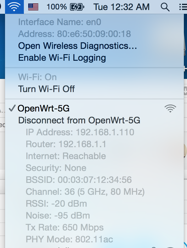
You’ll need a TFTPD server running on 192.168.1.100 to push files over. My Mac no haz ethernet (and Thunderbolt to Ethernet is crud), so I use my venerable X40 and tftpd software.
Firmware is up here. (Or you can compile your own) -> http://pan.baidu.com/s/1hqkVOfa
Firmware locations in flash (see below)
printenv

bootargs=console=ttyS0,115200 root=31:02 rootfstype=jffs2 init=/sbin/init mtdparts=ath-nor0:256k(u-boot),64k(u-boot-env),6336k(rootfs),1408k(uImage),64k(mib0),64k(ART)

bootcmd=bootm 0x9f020000

bootdelay=1

baudrate=115200

ethaddr=0xba:0xbe:0xfa:0xce:0x08:0x41

ipaddr=192.168.1.111

serverip=192.168.1.100

dir=

lu=tftp 0x80060000 ${dir}u-boot.bin&&erase 0x9f000000 +$filesize&&cp.b $fileaddr 0x9f000000 $filesize

lf=tftp 0x80060000 ${dir}db12x${bc}-jffs2&&erase 0x9f050000 +0x630000&&cp.b $fileaddr 0x9f050000 $filesize

lk=tftp 0x80060000 ${dir}vmlinux${bc}.lzma.uImage&&erase 0x9f680000 +$filesize&&cp.b $fileaddr 0x9f680000 $filesize

stdin=serial

stdout=serial

stderr=serial

ethact=eth0
Environment size: 686/65532 bytes
Upload to the uBoot
U-Boot 1.1.4--LSDK-10.1.389 (Apr 9 2014 - 15:23:02)
U-Boot DB120
Wasp 1.2
DRAM: 64 MB
Flash Manuf Id 0xef, DeviceId0 0x40, DeviceId1 0x17
flash size 8MB, sector count = 128
Flash: 8 MB
Using default environment
In: serial
Out: serial
Err: serial
Net: ag934x_enet_initialize...
No valid address in Flash. Using fixed address
No valid address in Flash. Using fixed address
wasp reset mask:c02200
WASP ----> S27 PHY
s27 reg init
: cfg1 0x80000000 cfg2 0x7114
eth0: ba:be:fa:ce:08:41
athrs27_phy_setup ATHR_PHY_CONTROL 4 :1000
athrs27_phy_setup ATHR_PHY_SPEC_STAUS 4 :10
eth0 up
WASP ----> S27 PHY
s27 reg init lan
ATHRS27: resetting s27
ATHRS27: s27 reset done
: cfg1 0x800c0000 cfg2 0x7214
eth1: ba:be:fa:ce:08:41
athrs27_phy_setup ATHR_PHY_CONTROL 0 :1000
athrs27_phy_setup ATHR_PHY_SPEC_STAUS 0 :10
athrs27_phy_setup ATHR_PHY_CONTROL 1 :1000
athrs27_phy_setup ATHR_PHY_SPEC_STAUS 1 :10
athrs27_phy_setup ATHR_PHY_CONTROL 2 :1000
athrs27_phy_setup ATHR_PHY_SPEC_STAUS 2 :10
athrs27_phy_setup ATHR_PHY_CONTROL 3 :1000
athrs27_phy_setup ATHR_PHY_SPEC_STAUS 3 :10
eth1 up
eth0, eth1
Setting 0xb8116290 to 0x30602d0f
Autobooting in 1 seconds
db12x>
db12x> tftpboot 0x81000000 image.bin
eth1 link down
enet0 port4 up
dup 1 speed 100
Using eth0 device
TFTP from server 192.168.1.100; our IP address is 192.168.1.111
Filename 'image.bin'.
Load address: 0x81000000
Loading: #################################################################
#################################################################
#################################################################
#################################################################
#################################################################
#################################################################
#################################################################
#################################################################
#################################################################
##############################
done
Bytes transferred = 3145732 (300004 hex)
db12x> erase 0x9f020000 +0x3c0000
Erasing flash... ............................................................
Erased 60 sectors
db12x> cp.b 0x81000000 0x9f020000 0x3c0000
Copy to Flash... ............................................................done
db12x> bootm 9f020000
It should boot into OpenWRT, you can flash from there.
...[long kernel bootlogs redacted]
- init complete -
BusyBox v1.22.1 (2014-12-15 18:46:26 CST) built-in shell (ash)
Enter 'help' for a list of built-in commands.
_______ ________ __
| |.-----.-----.-----.| | | |.----.| |_
| - || _ | -__| || | | || _|| _|
|_______|| __|_____|__|__||________||__| |____|
|__| W I R E L E S S F R E E D O M
-----------------------------------------------------
BARRIER BREAKER (14.07, r42625)
-----------------------------------------------------
* 1/2 oz Galliano Pour all ingredients into
* 4 oz cold Coffee an irish coffee mug filled
* 1 1/2 oz Dark Rum with crushed ice. Stir.
* 2 tsp. Creme de Cacao
-----------------------------------------------------
cat /proc/mtd
dev: size erasesize name
mtd0: 00020000 00010000 "u-boot"
mtd1: 0010206c 00010000 "kernel"
mtd2: 006cdf94 00010000 "rootfs"
mtd3: 004d0000 00010000 "rootfs_data"
mtd4: 00010000 00010000 "art"
mtd5: 007d0000 00010000 "firmware"
I highly recommend replacing the bootloader with an unlocked one.
i.e. this one – https://github.com/pepe2k/u-boot_mod
Bootloader sits at 0x9f000000 and is 64kb in size.
Suggest load in ram at 0x80060000 like they do, and flash from there.
eg from the bootloader –
tfpboot 0x80060000 uboot.bin

erase 0x9f000000 +0x20000

cp.b 0x80060000 0x9f000000 0x20000
Pray that it didn’t mess up (or you need an spi flasher…), and reboot!
Other bits n bobs –
You’ll need to adjust the opkg.conf file
ssh into the router @ 192.168.1.1 / root / root
mv /etc/opkg.conf /etc/opkg.conf.orig
echo 'dest root /
dest ram /tmp
lists_dir ext /var/opkg-lists
option overlay_root /overlay
src/gz barrier_breaker_base http://downloads.openwrt.org/barrier_breaker/14.07/ar71xx/generic/packages/base
src/gz barrier_breaker_management http://downloads.openwrt.org/barrier_breaker/14.07/ar71xx/generic/packages/management
src/gz barrier_breaker_oldpackages http://downloads.openwrt.org/barrier_breaker/14.07/ar71xx/generic/packages/oldpackages
src/gz barrier_breaker_packages http://downloads.openwrt.org/barrier_breaker/14.07/ar71xx/generic/packages/packages
src/gz barrier_breaker_routing http://downloads.openwrt.org/barrier_breaker/14.07/ar71xx/generic/packages/routing
src/gz barrier_breaker_telephony http://downloads.openwrt.org/barrier_breaker/14.07/ar71xx/generic/packages/telephony
src/gz barrier_breaker_luci http://downloads.openwrt.org/barrier_breaker/14.07/ar71xx/generic/packages/luci
#src/gz barrier_breaker_base http://downloads.openwrt.org/snapshots/trunk/ar71xx/packages/base
#src/gz barrier_breaker_management http://downloads.openwrt.org/snapshots/trunk/ar71xx/packages/management
#src/gz barrier_breaker_oldpackages http://downloads.openwrt.org/snapshots/trunk/ar71xx/packages/oldpackages
#src/gz barrier_breaker_packages http://downloads.openwrt.org/snapshots/trunk/ar71xx/packages/packages
#src/gz barrier_breaker_routing http://downloads.openwrt.org/snapshots/trunk/ar71xx/packages/routing
#src/gz barrier_breaker_telephony http://downloads.openwrt.org/snapshots/trunk/ar71xx/packages/telephony' >> /etc/opkg.conf
…and install Luci (the openwrt webui)
opkg update

opkg install luci
You should be able to visit http://192.168.1.1 and start changing settings.
Had an interesting issue trying to install/upgrade to Mavericks on an Apple 4,1 Mac Pro Desktop.
It was running Snow Leopard, but if I tried to install Mountain Lion or Mavericks it would give a disk error on reboot into the installer.
I made a USB installer, booted off that, and could see that disk utility couldn’t see any drives inside the installer.
As the equipment was working fine on Snow Leopard, this wasn’t a hardware issue.
I updated the firmware on the machine to the latest version, but still the same issue.
Cleared NV ram, same.
Compared SMC revisions, AHCI firmware revisions against a good machine, everything was the same.
Checked dmesg on the machine during a Mavericks installer boot, and could see that it was having issues with wifi, then with SATA.
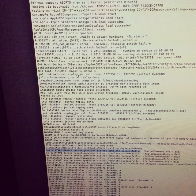
I checked the other machine, and saw that it had a different wifi card. Bingo!
I removed the wifi card from the non-working machine, and rebooted back into the installer, and it could suddenly see the drives again.
My conclusion is that the Intel ACH10 drivers, and the Atheros ARB5X86 drivers conflict with each other in 10.8 and above. I tested in the 10.10 beta too to be sure, and had the same issue.
Something apple needs to sort out, I guess..
Interesting issue, it took me a little while to troubleshoot.
We often have clients that complain about wifi in different area’s of their apartment being weak.
While there are a number of solutions to that, such as running additional cabling, adding additional routers via WDS, using 电力猫 (ethernet over power) adaptors etc, we decided to try out a newish all in one solution from TP Link.
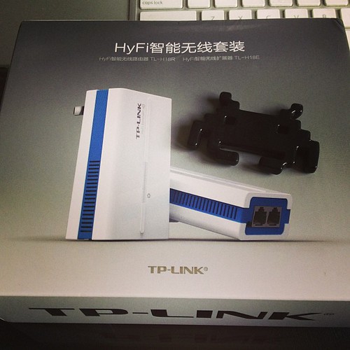
This ties together 2 paired mini wifi routers via power over ethernet (HomeAV).
See the Chinese diagram below for a clear example.
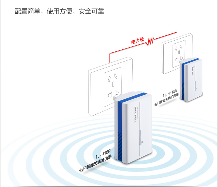
What does it do?
Well, you can plug one router in where your internet connection is, then plug the other router where your signal isn’t 😉 With a bit of luck, it will connect successfully over your power lines automagically, and there is no configuration needed other than adding in your internet settings at the router side.
The units provide both Ethernet and Wifi at both ends, so they’re a good solution for both wired and wireless access.
The units we bought only have Chinese firmware at the moment, but its pretty much set, and forget for most users.
They also come reasonably well documented – each unit has a sticker with its ip address and user/pass. Yay!
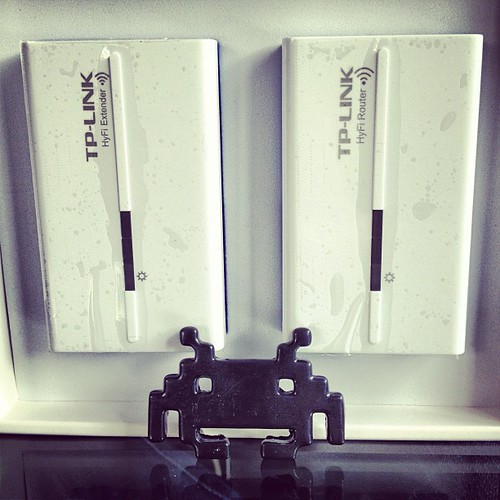
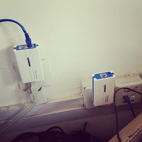
As you can see below, one unit has 2 ethernet connectors, and the other has 1 ethernet connector.
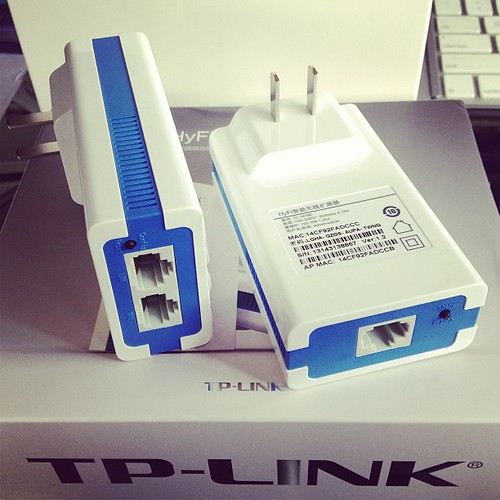
The unit with 2 connectors sits at your modem side (it can also extend an existing network if you have another wifi router already).
The WAN port plugs into your modem or network (as appropriate for your needs).
The LAN port provides a network port for use.
The other unit plugs in elsewhere (eg in a suitable location where you need wifi or wired connection).
I initially thought our initial unit was faulty, as it would only pair to the second adaptor for a few seconds, then stop pinging its ip address (192.168.1.254 as per its label)
–
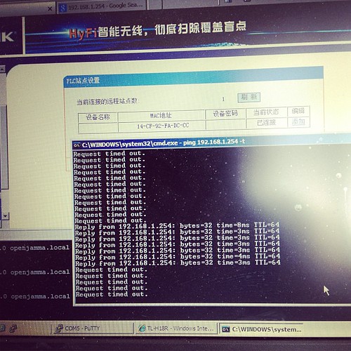
Turns out that once its booted up and paired, it gets an address via DHCP from the main
device, so whats written on the back of the unit no longer applies. Stumped me for a few seconds till I realised and went doh!
Here is our suitable test bed.
I’m pinging one device from the other –
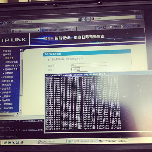
..and it works.
The units are a bit flimsy, but seem to work fine in our limited testing.
Price – RMB258 + shipping for a paired set via http://tp-link.tmall.com/ online store (price correct at time of writing)
Extra units – RMB133 (you can have up to 7 units tied together to extend your network).
I’d give these a rating of 7/10 – they’re cheap, and they work.
Further reading (and tools):
http://www.zibri.org/2009/03/powerline-ethernet-fun-and-secrets.html
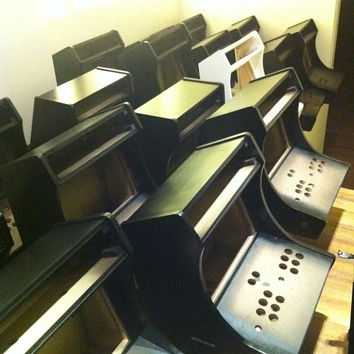
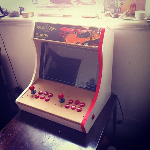
As visitors to my office have noticed, we’ve been building a bunch of arcade machines for clients.
Here are a couple of pics of the builds in progress:
Chassis’s undergoing painting
Unfinished machine
While making those is fun, I also have an interest in what powers them.
Arcade Machines are really just a wooden box, a display, a controller board, input (buttons and joysticks), and a PSU, they’re pretty basic devices. There is an industry cabling standard – JAMMA which makes connecting them up nice and easy.
China has a number of hardware choices for powering them, ranging from PC based boards, original arcade boards, and what I think is the better solution for older games – emulation under embedded ARM/MIPS, vs dedicated boards.
We went through a number of different versions of hardware available here until I found something I liked.
Our currently build hardware du jour runs off of something called “King of Game”.
As is usual in China, no documentation, and the factory is less than forthcoming with information.
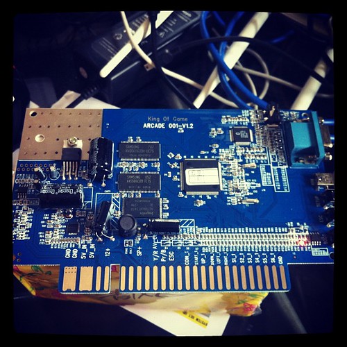
Still, not unusual.
The device does have some interesting features for the would be hacker –
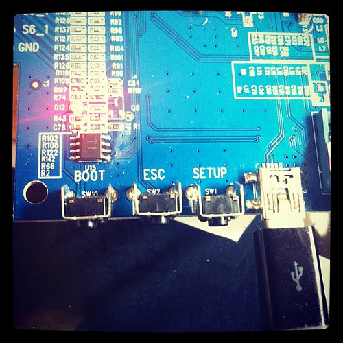
It has a nicely labelled “Boot” button, and the component count is quite low. Which generally means its SoC (System on a Chip) based.
The factory has done a little bit of prep work in making sure us ev1l hackorz won’t get at the juicy bits by etching off the cpu.
A quick look at the chip pin count, and the usual choice of chipset SoC more or less got me the right answer in a few minutes though.
My guess was Ingenic 4850, and it turned out to be the Ingenic 4755. This is a MIPS based X-Burst CPU
Even though they’re Chinese vendor, Ingenic does a great job in providing readily available information about their chipset(s). Kudos to the Ingenic guys in Beijing for being so open!
Datasheets for the 4755 and more importantly toolchains are readily available at the Ingenic FTP site – ftp://ftp.ingenic.cn/2soc/4750
Back to the board.
The King of Game board has USB onboard.
Plugging it into a computer shows the flash files available, but unfortunately not the firmware bits I need to see / change (e.g. to upgrade emulator capabilities, and change graphics).
If I hold down boot and plug in the USB, I get prompted for the Ingenic 4750 drivers.
Those are relatively easy to find on the ingenic site, so get a hold of those yourselves.
In order to connect to the board, you use a USB_BOOT.exe (there are also Linux tools available).
I downloaded usbboot-1.4b usbboot1.4b-tools, and unzipped that.
The USB Boot file needs a config file though – and the default config files supplied didn’t work 🙁
So, off to check what could be up.
The USB_Boot utility requires a bunch of settings in order to communicate with a board. After a bit of fiddling playing around with possible options I got it talking to the board.
While I’m not certain I have the settings completely correct here is what I have right now:
[PLL]
EXTCLK 24 ;Define the external crystal in MHz
CPUSPEED 336 ;Define the PLL output frequency
PHMDIV 3 ;Define the frequency divider ratio of PLL=CCLK:PCLK=HCLK=MCLK
BOUDRATE 57600 ;Define the uart boudrate
USEUART 0 ;Use which uart, 0/1 for jz4740,0/1/2/3 for jz4750
[SDRAM]
BUSWIDTH 16 ;The bus width of the SDRAM in bits (16|32)
BANKS 4 ;The bank number (2|4)
ROWADDR 12 ;Row address width in bits (11-13)
COLADDR 9 ;Column address width in bits (8-12)
ISMOBILE 0 ;Define whether SDRAM is mobile SDRAM, this only valid for Jz4750 ,1:yes 0:no
ISBUSSHARE 1 ;Define whether SDRAM bus share with NAND 1:shared 0:unshared
[NAND]
BUSWIDTH 8 ;The width of the NAND flash chip in bits (8|16|32)
ROWCYCLES 3 ;The row address cycles (2|3)
PAGESIZE 2048 ;The page size of the NAND chip in bytes(512|2048|4096)
PAGEPERBLOCK 64 ;The page number per block
FORCEERASE 0 ;The force to erase flag (0|1)
OOBSIZE 64 ;oob size in byte
ECCPOS 6 ;Specify the ECC offset inside the oob data (0-[oobsize-1])
BADBLACKPOS 0 ;Specify the badblock flag offset inside the oob (0-[oobsize-1])
BADBLACKPAGE 127 ;Specify the page number of badblock flag inside a block(0-[PAGEPERBLOCK-1])
PLANENUM 1 ;The planes number of target nand flash
BCHBIT 4 ;Specify the hardware BCH algorithm for 4750 (4|8)
WPPIN 0 ;Specify the write protect pin number
BLOCKPERCHIP 0 ;Specify the block number per chip,0 means ignore
[END]
If I put the board into USB boot mode (hold down boot button, and plug into the usb), then run the USB_TOOL.EXE file I can communicate
 Welcome!

 USB Boot Host Software!

 USB Boot Software current version: 1.4b

 Handling user command.

 USBBoot :> list
Device number can connect :1
USBBoot :> help
Command support in current version:
help print this help;
boot boot device and make it in stage2;
list show current device number can connect;
fconfig set USB Boot config file;
nquery query NAND flash info;
nread read NAND flash data with checking bad block and ECC;
nreadraw read NAND flash data without checking bad block and ECC;
nreadoob read NAND flash oob without checking bad block and ECC;
nerase erase NAND flash;
nprog program NAND flash with data and ECC;
nmark mark a bad block in NAND flash;
go execute program in SDRAM;
version show current USB Boot software version;
exit quit from telnet session;
readnand read data from nand flash and store to SDRAM;
load load file data to SDRAM;
run run command script in file;
memtest do SDRAM test;
gpios let one GPIO to high level;
gpioc let one GPIO to low level;
sdprog program SD card;
sdread read data from SD card;
USBBoot :> boot
Usage: boot (1)
1:device index number
USBBoot :> boot 0
Checking state of No.0 device: Unboot
Now booting No.0 device:
Download stage one program and execute at 0x80002000: Pass
Download stage two program and execute at 0x80c00000: Pass
Boot success!
Now configure No.0 device:
Now checking whether all configure args valid:
Current device information: CPU is Jz4750
Crystal work at 24MHz, the CCLK up to 336MHz and PMH_CLK up to 112MHz
Total SDRAM size is 16 MB, work in 4 bank and 16 bit mode
Nand page size 2048, ECC offset 6, bad block ID 127, use 1 plane mode
Configure success!
Next up, read the firmware off the flash, and dump it to see which version of the Dingoo code they most probably ripped off 🙂
31
Kudelski N3 bits and pieces.
Kudelski N3 bits and pieces, plus thoughts on key / rsa extraction from flash.
N3 Notes mostly from forum posts by TheCoder
These are notes for future reference more than anything else, so please no excited emails about how its wrong, or right, or can I hack your box.
—
There are three different pairing methods used N3 boxes presently. These are DT06, DT08 and Secondary key.
The DT06 method transfers a compressed form of an rsa pq keyset from which the CAM public/private rsa keyset and its associated modulus can be derived.
The DT08 method transfers the cam modulus along with the IRD number of the married box. The public rsa key is not transferred but it is implied that the box already knows this value.
The Secondary key method does not involve a transfer. It imples that the box already knows the cards matching CAM modulus and rsa public key value.
Various boxes, depending on make/model, may use any of the above pre-pair key transfer methods but it could be useful to know which box uses which method.
http://www.digital-kaos.co.uk/forums/f10/people-n3-cards-82421/
Instructions:
1 Stick your N2/N3 card in your card reader
2 Run NagraEdit – DO NOT ATTEMPT TO READ YOUR CARD !!!
3 Select the Comm Tab. This should give you an upper and lower text pane
4 Cut/Paste the scriptt below into the top pane
5 Press the “Send D2C” button/icon
6 Results should appear in bottom pane
7 Interpret your results based on info below.
Script – Read DT06/DT08
Code:
rs
tx 21 C1 01 FE 1F
rx
tx 21 00 08 A0 CA 00 00 02 12 00 06 55
dl 02 00
rx
dl 02 00
tx 21 00 09 A0 CA 00 00 03 22 01 00 1C 7E
dl 02 00
rx
dl 02 00
mg *
mg *** DT06 info ***
tx 21 00 09 A0 CA 00 00 03 22 01 06 13 **
dl 02 00
rx
mg DT06 response1
dl 02 00
tx 21 40 09 A0 CA 00 00 03 22 01 86 13 **
dl 02 00
rx
dl 02 00
mg DT06 response2
mg *** End DT06 info ***
mg *
mg *** DT08 info ***
tx 21 40 09 A0 CA 00 00 03 22 01 08 13 **
dl 02 00
rx
mg DT08 response1
dl 02 00
tx 21 00 09 A0 CA 00 00 03 22 01 C8 55 **
dl 02 00
rx
dl 02 00
mg DT08 response2
tx 21 40 09 A0 CA 00 00 03 22 01 88 55 **
dl 02 00
rx
mg DT08 response3
dl 02 00
mg *** End DT08 info ***
*******
Just to clarify :
The important bits your looking at are the DT06/DT08 responses (the bits that start with Rx: )
ie RX: 12 00 15 A2 11 08 E0 00 00 00 5E 01 20 00 00 00
00 00 00 00 00 00 90 00 B3
RX: 12 40 15 A2 11 00 00 00 00 00 00 00 00 00 00 00
00 00 00 00 00 00 90 00 64
RX: 12 00 15 A2 11 00 00 00 00 00 00 00 00 00 00 00
00 00 00 00 00 00 90 00 24
and
RX: 12 40 57 A2 53 00 00 00 00 00 00 00 00 00 00 00
00 00 00 00 00 00 00 00 00 00 00 00 00 00 00 00
00 00 00 00 00 00 00 00 00 00 00 00 00 00 00 00
00 00 00 00 00 00 00 00 00 00 00 00 00 00 00 00
00 00 00 00 00 00 00 00 00 00 00 00 00 00 00 00
00 00 00 00 00 00 00 00 90 00 64
If the responses vary significantly from the above, with the 00’s replaced with some varying data, then its likely your card had the specified tier and is probably using the corresponding pairing method.
If the DT06 response contains lots of 00’s then its NOT DT06 pairing
If the DT08 response contains lots of 00’s then its NOT DT08 pairing
If its not DT06 or DT08 then its probably secondary key.
For non DT08 cards (mostly the newer boxes) each box has a unique cam_n already built into its firmware – this can only be extracted from the actual box itself.
About the Algorithm,
N2 encrytion was based on the following algorithm ->
decrypted message = ( (IDEA( ( (EncryptedMsg ^ 3)Mod N1) ,IdeaKey) ) ^3) Mod N1
Thats 2 distinct algorithms. An RSA algorithm (performed twice) and an IDEA algorithm.
The key for the RSA algorithm is something like –
RSA EMM-G=15A811B2065DF39CD48C9C958E7B406345295B09D0E9A18A 9B92C5FD7761CAAFAB830880F1F06B4E4477F157EA10D0AFC3 FDDB1ED2E7E83E89F03FF81237047DB76F79D6A2CFD75A7255 D72E52E7F47B96C2DFBDEBFC80CE927F6AD351FDF0BF8DA13F F62295BFBAF29035A230136D0B4AA99D38DD8B0465F2C709FC 8818173C
Which, as you can see, is a 128 byte (1024 bit) number. This is the main encryption key for EMM decryption.
The IDEA algorithm, which acts as an inner layer to the RSA has a standard 16 byte (128 bit) IDEA key.
There is no algorithm in N2 (or N3) that only uses an 8 byte (64 bit) key although some providers have opted to use 3DES rather than IDEA as an inner layer. This uses three separate 8 bye (64 bit – only 56 bits used) keys to form an amalgam 168 bit DES algorithm.
If Using DT08 (0a) on the card :
The Dt08 (0a datatype on card) is created by the provider and sent to the card at sub time.
The dt08 contains the Cam N public rsa key along with ird/boxkey.
The dt08 is IDEA encrypted with the Idea Key made from ird/boxkey/inverted ird.
The dt08 is RSA encrypted using Ird N (public rsa key) and Ird D (private key and uknown by anyone but provider).
Ird N = N1 xored N2
Ird N1= A4E9B585932F90282FD70C908176E8605E6B2CE629335A0FC1 5B31DAB0BFC6FEEB88CFC69649994CD3FE039C9965C620C4D5 828E9153998EE4AE0E8C25644DF3 xor
Ird N1= 237280AAB36BE4B21FC71FBF08218E532A545E744D7B007FF8 69BA426831C4AC653F3825ADE9358FCD1F0239EC447CBC2765 CC0AEBE437AF2270FC461C2FA042
Ird N = 879B352F2044749A3010132F89576633743F729264485A7039 328B98D88E02528EB7F7E33BA0ACC31EE101A57521BA9CE3B0 4E847AB7AE21C6DEF2CA394BEDB1
The Ird N1,N2,Ideakey exist in the tsop.
Ird E = 3
Ird D = UKNOWN, this is the reason you can’t create your own dt08 without changing the N1/N2 on the tsop, you must know Ird D.
DT08 (0A) = IdeaEncrypt(CamN/Ird#/Boxkey/Idea Signature,Ird_Ideakey) ^ D mod Ird N.
Ird requests DT08.
Card sends back the dt08 (0a)
Ird decrypts the dt08.
Decrypted dt08 = IdeaDecrypt(DT08,Ird_IdeaKey) ^ 3 mod Ird N.
It checks the ird # and boxkeys in the Decrypted 08 if they match what is on ird,
it stores the Cam N in the decrypted 08 in ird memmory.
If Using Secondary Key (SK) on the Ird.
Ird checks for SK exists on the ird, if it does, the dt08 will never be requested/ignored from the card.
Ird validates the SK with idea signature in the SK (using IIIIIIII01924314051647990A9C4E1 where I = irdnumber).
Ird takes the Cam N in the SK and puts it in ird memmory
Note : Cam N is not even encrypted in the sk, very weak method compared to dt08.
Later, establish session key (0C datatype on the card):
Ird requests 2a data from card.
Random 2a is sent from card to ird.
Ird performs some Idea signing (leave it to you to look up 2a/2b routines)
Ird comes up with session key from the 2a message sent from Cam.
Ird encrypts the session key with rsa.
Encrypted 2B = (2B data with 16 byte session idea key) ^ 3 mod Cam N.
Sends encrypted data back to card in 2b message.
Cam decrypts 2B with Cam N, Cam D. Decrypted 2B = (Encrypted 2B) ^ Cam D mod Cam N.
If valid, store session key in ram and on card for later use.
This all happens as ird boots.
When you select a channel.
Ird sends Cmd 07 ECM message with control words encrypted.
Cam decrypts the control words rencrypts them with Idea encryption using the session key established above.
The ird then requests the control words.
The Cam sends them back in the 1C response.
The ird decrypts the control words with with Idea encryption using the session key established above.
Sends the control words to the mpeg decoder.
8 seconds of video.
Repeat 07/1C process over and over.
——–
and pay special attention on CMD$2A ??
it should reply the CAMID serial number + 64 bytes random key generated and then shortly after encrypted with the CAM(AKA Conditional Access Module or SmartCard) RSA primary 96 bytes from the card… the so famous RSA modulus keys 96bytes at eeprom $8xxx on the ROM110 days.. From the card (this cmd is also the first step of the SessionKey negotiation)
shortly after the receiver receives this card reply.. and will decrypt it using the Secondary Key which is also 96bytes, this key is build up by using the following information stored in the receivers flash..
IR IR IR IR ZZ ZZ ZZ ZZ ZZ ZZ ZZ ZZ 00 03 F1 F1
F1 F1 F1 F1 F1 F1 SK SK SK SK SK SK SK SK SK SK
SK SK SK SK SK SK SK SK SK SK SK SK SK SK SK SK
SK SK SK SK SK SK SK SK SK SK SK SK SK SK SK SK
SK SK SK SK SK SK SK SK SK SK SK SK SK SK SK SK
SK SK SK SK SK SK F2 F2 F2 F2 F2 F2 F2 F2 CR CR
total 96 bytes..
IR = Receiver serial number
XX = Unimportant
EE = RSA public exponent for STB
F1 = SK signature 1 used to calculate the box key
F2 = SK signature 2 used to calculate the box key
SK = RSA public modulus N
CR = CRC Checksum
BB = BoxKey result from xoring F1 with F2 keys stored in the flash firmware from the receiver
once we decrypt the cmd2A we extract from inside the original 64byte random key generated in the card, then we will apply the IDEA encryption algo on the first 32bytes from the 64 byte random key to hash out the session key.
So this first 32 bytes are extracted from the 64byte random key and will be encryted using the IDEA SIGNATURE key… this key will be generated by the following information
IdeaKey generation
BB BB BB BB BB BB BB BB + CC CC CC CC + CA MI DC AM
BBBBBBBBBBBBBBBB = Boxkey result from F1 xor F2
CCCCCCCC = IRD number from receiver stored in Flash firmware
CA MI DC AM = CAM ID or Smart Card serial number converted in HEX, which can also be extracted by simply sending INS CMD$12 to the card..
so the IDEA signature key for encrypting the first 32bytes extracted from the 64 random seek key is
BBBBBBBBBBBBBBBBCCCCCAMIDCAM
once applied the IDEA encryption we will have the result 16 byte sessionkey.. which will be stored in the receiver flash for a few hours… to be more precise around 5 hours..
Now going back to the calculation done before, the receiver decrypted the cmd$2Aencrypted by the card with the RSA primary 96 stored in the card.
once decrypted it simply just extracted the first 32bytes of the 64 byte seed key generated by the card. this 32 bytes were used for calculation of the 16byte sessionkey..
but, before the 32byte keys was taken for the idea signature encryption.. the receiver.. re-encrypted the 64byte random key using the SECONDARY KEY RSA 96 stored in the receiver flash, which i just stated above how to get this key…
and will send it back to the card on cmd$2B
the card will receive the cmd$2b and will decrypt it using the PRIMARY RSA modulus key 96.
and will extract just the first 32bytes.. and by using the BOXKEY+IRD+CAMID stored in the card, the card will also calculate the same 16 byte session key.
in orde to make the card pairing , u need to know the RSA_N+BOXKEY+IRD NUMBER+CARD SERIAL number or CAMID…
then with them all together we can start comunication between the card.. and on the CMD$2A and $2B we will have the SessionKey negotiation which i just explained previously.
if for example on one side or the other we have different BKand RSA… we will a session key failure.. and without this Sessionkey we will not be able to decrypt the CM$1C or $9C related stuff
this means that if negotiation of session key succeds, then the receiver will send the ECM$07 to the card, which will then be decrypted by simply just using the ECM RSA modulus key and the ECM IdeaKey to decrypt the Control Words / CWs.
once they are decrypted the card will send them to the RECEIVER.. this is normally done via CMD$1C obviously this CMD is encrypted with the Sessionkey 16 BYTES described above.. once it arrives at the Receiver end, you will use the same Sessionkey 16byte to decrypt that CMD$1C and extract the REAL DCWs Decrypted Control Words to open up the Video and Audio stream related for that XX amount of seconds…
Now this Session key is refreshed every 5 hours.. this means that every 5 hours a new session key is produced.. so every 5 hours the card generates another 64byte random seed key using other RSA algo inside the card.., and will then send this 64 byte seed key to the receiver again.
Shortly followed by all the procedure described above to extract the new session key again.
—————-
Given that ==================================================
SK 96 BYTES
==================================================
11111111<----------------------------FIRST 4 BYTES---- IRD
XXXXXXXXXXXXXXXXXXXX<--NEXT 10 BYTES---- unknown
1111111111111111<--------8 BYTES---- Y1---WRITE DOWN
==================================================
11111111111111111111111111111111-_
11111111111111111111111111111111-_-_"N" 64 Bytes
11111111111111111111111111111111-_-
11111111111111111111111111111111-
==================================================
1111111111111111<-------8 BYTES--- Y2-----WRITE DOWN
XXXX<-------------------2 BYTES--- CHECKSUM
==================================================
Y2 Xor Y1 = BOXKEY
==================================================
006e convert from hex gives you 110 bytes block cipher
ird 4 bytes
bk 8 bytes
sk 96 bytes
leaving us with 02bytes used to encrypt, decrypt above.
eg:
00 00 00 6e 34 0d 20 1c 03 03 70 80 5a 8e dd 24
ac cc a4 a6 e2 da 86 91 29 18 0b a6 23 6d fa c4
05 7f 1b 20 97 eb 0c 19 b3 39 2f 1e cb 9b 67 4d
ed 10 f5 65 ec 0d c7 35 ac f0 b8 89 b0 51 59 22
69 85 d5 f1 93 48 7a 84 6e 1f b4 24 83 79 db 02
4d b0 9c 5e 8b df 89 57 9c 5a 7f 9a cc 87 51 3b
15 6b 15 cc c4 2f 66 e7 e6 75 4f 24 f2 07 85 0d
db b0 3d e2 64 dd e9 54 ad 77 60 e7 8f a6 cd a6
46 c3 b8 fa e4 e7 51 2d 6a 2f 95 68 56 b5 78 34
17 6b b8 48 38 87 c4 95 e5 b0 41 2c 95 e1 24 aa
4b 2a 6f 8c 90 53 29 a9 6b 3d 0a b5 92 1c 95 ec
72 b9 54 a9 99 f5 f3 dd f4 0f 60 c3 25 5b 5b 81
22 e8 79 c5 be 8f 3c 89 2b 8a ad ba 27 b0 c2 f7
b1 4f 08 d5 37 2a 97 c5 f0 07 9d 99 be c7 8a a9
cf 5a c5 45 ce 1e 25 43 81 95 7a 22 33 ed 93 74
Gives:
00 00 00 63 (length)
0d 20 1c 03 03 70 80 5a 8e dd (unknown)
24 ac cc a4 a6 e2 da 86 (y1)
91 29 18 0b a6 23 6d fa c4
05 7f 1b 20 97 eb 0c 19 b3 39 2f 1e cb 9b 67 4d
ed 10 f5 65 ec 0d c7 35 ac f0 b8 89 b0 51 59 22
69 85 d5 f1 93 48 7a 84 6e 1f b4 24 83 79 db 02
4d b0 9c 5e 8b df 89 (64 bytes)
57 9c 5a 7f 9a cc 87 51 (y2)
Y2 XOR Y1 = 0x579c5a7f9acc8751 xor 0x24accca4a6e2da86 = 42 12 8C F2 39 39 55 FA
So, a flash dump would be helpful..
Possible Scenario's -
BGA, TSOP, TLGA etc.. desoldering for Flash.
Put in a socket. eg from
http://shop37051047.taobao.com/ or http://shop34694309.taobao.com/?search=y
Pop flash back onto something else, read, dump. eg
http://item.taobao.com/item.htm?id=7422440993
Get box key, rsa key (if req. based on a check of DT type from the actual subbed card)
Pop flash back in socket.
Been there, done that for data recovery on faulty flash drives, plus most of the places I know down at QJlu have SMD / BGA desoldering capability or better.
Bunnies blog is fairly good at explaining the basics (albeit for xbox) – http://www.xenatera.com/bunnie/proj/anatak/xboxmod.html
Most boxes use ARM based SoC’s for things. Also possible to just throw up a dev board, and interface to that.
Although most boxes also have some form of OS running, so just as feasible to dump flash that way also assuming serial or jtag access and a bootloader is available.
Amusing that people like http://www.flashbackdata.com/blog/?p=195 claim this is hard – there are plenty of tools for this already out there eg softcenter, pc3000, plus all the local chinese stuff. Semi ok forum here talking about flash recovery, although not as technical as I’d like.
http://forum.hddguru.com/hard-disk-drives-english-forum-f12.html
Once key(s) are had, then I can use my own decoder rather than the crappy one the broadcaster uses.
Yay.
Had a client come into the office today with a locked iPhone.
Normally this isn’t really a big deal (assuming that there is a hack for it), but in this case, it was a little more complex, as he didn’t have working wifi.
PwnageTool has a great feature where you can add Cydia Packages to a custom firmware, so that you can prepackage the firmware already to go.
So, I opened up PwnageTool, added the http://repo666.ultrasn0w.com/ site to the Cydia sources section in advanced, and tried to load in Ultrasn0w.
Life isn’t easy, and it didn’t work.
But why didn’t it work?
I took a look at a working site, and checked out the differences between their package section and Ultrasn0w’s.
Ultrasn0w is hosted on repo666.ultrasn0w.com
While their website doesn’t really tell you much useful information, a bit of googling lead to some info.
The .deb file (debian package file) on their site is at http://repo666.ultrasn0w.com/ultrasn0w.deb
Cydia usually needs stuff in a particular format, so I next checked out how one makes a repository.
This is documented at Saurik’s site here – http://www.saurik.com/id/7
Basically, you throw files into a folder and make a Packages file.
The example given on Saurik’s site is this:
/web/apt/xmpl]# dpkg-scanpackages -m . /dev/null >Packages

 ** Packages in archive but missing from override file: **

  com.saurik.myprogram
Wrote 1 entries to output Packages file.
[root@desktop:/web/apt/xmpl]# bzip2 Packages
[root@desktop:/web/apt/xmpl]# ls -la *
-rw-r--r-- 1 root root 906 2008-07-01 07:48 MyProgram.deb
-rw-r--r-- 1 root root 380 2008-07-01 08:00 Packages.bz2
[root@desktop:/web/apt/xmpl]#
So, it appears we need a Packages.bz2 file.
Being adventurous, I decided to setup my own repo, and stuck the .deb file for Ultrasn0w in there.
Followed the instructions and created the Packages.bz2 file.
Tried again in PwnageTool, and… No go.
Hmm.
Does http://repo666.ultrasn0w.com have a Packages.bz2 file?
Why yes it does.
Take another look at the working one – ahah says my brain.
They point the folder to the _uncompressed_ Packages file.
I guess PwnageTool doesn’t support compressed Package list files.
So, I try that out using an uncompressed file.
Created the Packages file with
dpkg-scanpackages -m . /dev/null >Packages
and try again.
Better – I’m getting a result now with my repo when I click refresh.
However, I can’t seem to be able to download any files…
So, lets take a look at whats happening in my apache logs.
58.37.213.199 - - [07/Mar/2011:20:50:52 +0800] "GET /dists/Packages HTTP/1.1" 200 1643 "-" "PwnageTool/4.2 CFNetwork/454.11.5 Darwin/10.6.0 (i386) (iMac9%2C1)"

58.37.213.199 - - [07/Mar/2011:20:51:06 +0800] "GET /./mobilesubstrate_0.9.3228-1_iphoneos-arm.deb HTTP/1.1" 404 1184 "-" "PwnageTool/4.2 CFNetwork/454.11.5 Darwin/10.6.0 (i386) (iMac9%2C1)"

58.37.213.199 - - [07/Mar/2011:20:51:42 +0800] "GET /./ultrasn0w.deb HTTP/1.1" 404 1164 "-" "PwnageTool/4.2 CFNetwork/454.11.5 Darwin/10.6.0 (i386) (iMac9%2C1)"
Aha! While its successfully found the repo now, its looking for the files in the wrong folder – my repo is in /dists, and its looking in the root folder.
Seems the Saurik instructions are a bit mangled, or the Package generator is a bit silly.
Quick look at the helpfile shows it needs the folder via -m
So I went up a level, and regenerated my file.
cd ..

dpkg-scanpackages -m dists > dists/Packages
Yes, it works!

Now PwnageTool can download my file finally. Yay!
I just need to select it in PwnageTool / Packages as below, and build my ipsw to test.

Now I can finally make my own Ultrasn0w firmware woohoo!
Not as hard as it seems, but not as easy either!
I’ll leave my UltraSn0w repo at http://www.sheed.com/dists/ for now, but will probably move it elsewhere at some point, and update this post. So, if you need it, get it while you can.
Lawrence.
Archives
- November 2024
- November 2019
- October 2019
- August 2019
- April 2019
- February 2017
- September 2016
- June 2016
- May 2016
- September 2015
- August 2015
- June 2015
- April 2015
- December 2014
- October 2014
- September 2014
- July 2014
- June 2014
- April 2014
- October 2013
- July 2013
- May 2013
- April 2013
- March 2013
- January 2013
- December 2012
- October 2012
- August 2012
- July 2012
- June 2012
- May 2012
- April 2012
- March 2012
- December 2011
- November 2011
- October 2011
- September 2011
- July 2011
- May 2011
- April 2011
- March 2011
- February 2011
- January 2011
- December 2010
- November 2010
- October 2010
- September 2010
- August 2010
- July 2010
- June 2010
- May 2010
- April 2010
- March 2010
- February 2010
- January 2010
- December 2009
- November 2009
- October 2009
- May 2009
- April 2009
- March 2009
- February 2009
- January 2009
- December 2008
- November 2008
- October 2008
- September 2008
Categories
- Apple
- Arcade Machines
- Badges
- BMW
- China Related
- Cool Hunting
- Exploits
- Firmware
- Food
- General Talk
- government
- IP Cam
- iPhone
- Lasers
- legislation
- MODx
- MySQL
- notice
- qmail
- requirements
- Reviews
- Service Issues
- Tao Bao
- Technical Mumbo Jumbo
- Things that will get me censored
- Travel
- Uncategorized
- Useful Info