Continuing on from my last post.
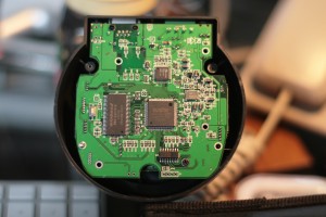
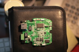
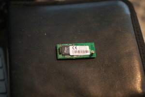
The board I have contains the following hardware (other than the CPU)
RAM – k4s561632d-tl75 = 16M X 8BITS x 2 banks (64m ram?)
ROM – H27UBG8T2A TR = 4G Nand Flash (4G MLC? some ref as 2G, need to double check..)
NAND Config:
1024 blocks. Each block has 256 programmable pages. Each Page is 8640 bytes (8192+448spare)
Ingenic has a USBBoot.exe tool which can be used to view the NAND.
Testing was done with these nand settings in usbboot.cfg:
[PLL]

EXTCLK            24            ;Define the external crystal in MHz

CPUSPEED        336            ;Define the PLL output frequency

PHMDIV            3            ;Define the frequency divider ratio of PLL=CCLK:PCLK=HCLK=MCLK

BOUDRATE        57600            ;Define the uart baudrate.  Yes they misspelt it.

USEUART            1            ;Use which uart, 0/1 for jz4740,0/1/2/3 for jz4750
[SDRAM]
;k4s561632d / : RA0 ~ RA12, Column address : CA 0 ~ CA 8
;32M x 2 chips = 64M total Ram.
BUSWIDTH 16 ;The bus width of the SDRAM in bits (16|32)
BANKS 4 ;The bank number (2|4)
ROWADDR 13 ;Row address width in bits (11-13)
COLADDR 9 ;Column address width in bits (8-12)
ISMOBILE 0 ;Define whether SDRAM is mobile SDRAM, this only valid for Jz4750 ,1:yes 0:no
ISBUSSHARE 1 ;Define whether SDRAM bus share with NAND 1:shared 0:unshared
[NAND]
BUSWIDTH 8 ;The width of the NAND flash chip in bits (8|16|32)
ROWCYCLES 3 ;The row address cycles (2|3)
PAGESIZE 8192 ;The page size of the NAND chip in bytes(512|2048|4096)
PAGEPERBLOCK 256 ;The page number per block
FORCEERASE 0 ;The force to erase flag (0|1)
OOBSIZE 448 ;oob size in byte
ECCPOS 0 ;Specify the ECC offset inside the oob data (0-[oobsize-1])
BADBLACKPOS 0 ;Specify the badblock flag offset inside the oob (0-[oobsize-1])
BADBLACKPAGE 0 ;Specify the page number of badblock flag inside a block(0-[PAGEPERBLOCK-1])
PLANENUM 2 ;The planes number of target nand flash
BCHBIT 4 ;Specify the hardware BCH algorithm for 4750 (4|8)
WPPIN 19 ;Specify the write protect pin number
BLOCKPERCHIP 0 ;Specify the block number per chip,0 means ignore
NAND Config notes –
HYNIX_H27UBG8T2AR 3.3V 32Gbit NAND
4096M x 8bit
ID of No.0 device No.0 flash: // ad d7 94 9a 74 42
Vendor ID :0xad (Hynix) //Manufacturer Code
Product ID :0xd7 (Device ID) // Device Identifier
Chip ID :0x94 //Internal Chip Number
Page ID :0x9a //Page Size/BlockSize/Redundant Area
Plane ID :0x74 //Plane Number , ECC
Tech ID :0x42 //Tech / EDO /Interface
3.3V Bus Width x8
3rd Byte Dev ID
0x94=0b10010100
00 – Internal Chip Number 1
01 – 4 Level Cell (cell type)
01 – 2 pages programmed at once
10 – Interleave supported, Write Cache Supported
0x9a=0b10011010
10 – 8kb page size
0 10 – 448 Bytes (redundant area size)
1 01 – 2M Block Size (without spare area)
0x74=0b 0 111 01 00
01 – 2 Planes
ECC level – reserved.
0x42=0b01 000 010
010 32nm Nand
0 EDO Supported
0 SDR NAND Interface
—-
I also see this though in one of the nand.cfg files
NandID,NandExtID=PlaneNum, Tals, Talh, Trp, Twp,Trhw, Twhr, dwPageSize, dwBlockSize, dwOOBSize, dwPageAddressCycle,dwMinValidBlocks,dwMaxValidBlocks, NandName
0xADD7,0x00749A94=1, 15, 5, 15, 15, 100, 80, 8192, 2048*1024, 448, 3, 1998, 2048, “HYNIX_HY27UBG8T2ATR”}
Its referred to there as a 2G sized chip. So.. are Hynix Docs right or the above?
—
A look at the NAND shows:
USBBoot :> nreadraw 0 1024 0 0
00000000 ff 55 55 55 55 55 55 55 ff ff ff ff 01 00 11 04 |.UUUUUUU……..|
00000010 00 00 00 00 21 e0 e0 03 00 00 e9 8f 21 e0 20 01 |….!…….!. .|
00000020 00 80 1d 3c 00 40 bd 37 00 80 19 3c 90 06 39 27 |…<.@.7...<..9'|
00000030 08 00 20 03 00 00 00 00 00 00 00 00 00 00 00 00 |.. .............|
00000040 1b 43 02 3c 83 de 42 34 19 00 82 00 0f 00 02 3c |.C.<..B4.......<|
00000050 10 20 00 00 40 42 42 34 82 24 04 00 1b 00 44 00 |. ..@BB4.$....D.|
00000060 f4 01 80 00 50 c3 03 34 21 60 a0 00 12 48 00 00 |....P..4!`...H..|
00000070 1b 00 69 00 f4 01 20 01 12 28 00 00 02 10 25 71 |..i... ..(....%q|
00000080 01 00 a4 24 50 c3 42 38 0b 28 82 00 04 00 a3 2c |...$P.B8.(.....,|
00000090 33 00 60 10 0c 00 a2 2c 04 00 05 24 fc ff a2 24 |3.`....,...$...$|
000000a0 40 23 02 00 20 4e 02 24 1b 00 49 00 f4 01 20 01 |@#.. N.$..I... .|
000000b0 12 28 00 00 04 00 a3 2c 27 00 60 14 c0 12 05 00 |.(.....,'.`.....|
000000c0 08 00 a2 2c 2a 00 40 10 00 18 8a 34 00 5a 05 00 |...,*.@....4.Z..|
….
Our JZ4755 is a MIPS XSCALE CPU.
The above dump is off of a NAND, so we have a 12byte prefix (need to look at the JZ dev nand.c for a proper reason why).
Allegedly in the spanish forums, its due to NAND write testing for signedness etc.
If I run it through a decompiler eg mips-linux-objdump -bbinary -mmips -D ..., I do see valid code, so our initial dump looks correct for MIPS.
MIPS == Backasswardness vs our dump, cough.
0: 555555ff 0x555555ff
4: 55555555 0x55555555
8: ffffffff 0xffffffff
c: 04110001 bal 14
10: 00000000 nop
14: 03e0e021 move gp,ra
18: 8fe90000 lw t1,0(ra)
1c: 0120e021 move gp,t1
20: 3c1d8000 lui sp,0x8000
24: 37bd4000 ori sp,sp,0x4000
28: 3c198000 lui t9,0x8000
2c: 273906b8 addiu t9,t9,1720
30: 03200008 jr t9
34: 00000000 nop
38: 00000000 nop
...
This should match up to our IPL -> SPL stuff uboot loader. Lets see, first though, an explanation.
IPL?
IPL = Initial Program Loader.
This is in CPU, and 8K in size (need to double check that in the Ingenic CPU docs), basically it boots to NAND, runs the code in NAND, unless otherwise directed via boot_sel.
Boot_Sel I hear you ask?
The JZ4755 has an integrated ROM with 8KB this memory is connected to the External Memory Controller (EMC).
After a processor reset, the processor runs the program contained in the ROM memory, and depending on the values of the boot_sel[1:0] flags carries out the following operations:
boot_sel[1:0]
00 Unused
01 Initialization via USB port: Receives a block of data through the USB (device) port,
and stores it in internal SRAM.
10 Initialization via NAND memory with 512-byte pages at Chip Select 1 (CS1):
11 Initialization via NAND memory with 2048-byte pages at Chip Select 1 (CS1):
Our CPU then reads the first byte from NAND to determine whether the bus is 8- or 16-bit.
(if bit[7:4] = 0, it is 16-bit), and the number of cycles per page is 2 or 3 (if bit[3:0] = 0, it is 2 cycles).
It then adjusts the EMC using this information and copies the first 8kB from NAND to the internal SRAM.
Our NAND has 8-bit data, 3 cyles, and 8192 bytes per page, so the first byte should be 0xFF
On our board, the boot_sel is configured by the cunningly labelled boot button.
If its pressed and we then connect a usb cable, our CPU then sits there waiting for an init via USB port.
So, we now know how the board boots up, and why our USB works.
So lets look at the actual boot code we decompiled above. Luckily I know a man with tar.gz roaming around the back streets, and persuaded him to give me some goodies. (Ok, fine, its all at the Ingenic.cn ftp site).
I’ll be even lazier though, and paste in the bits off of the Qi wiki here – http://en.qi-hardware.com/wiki/Boot_Process as its pretty much identical.
start.S
The first subroutine ran is the _start, which is defined in /cpu/mips/start.S, this subroutine makes a call to the reset function, defined on the same file, which code is shown next:
.globl _start
.text
.word JZ4740_NANDBOOT_CFG /*(0xffffffff) NAND 8 Bits 3 cycles */
b reset; nop /* U-boot entry point */
b reset; nop /* software reboot */
reset:
/*
* CU0=UM=EXL=IE=0, BEV=ERL=1, IP2~7=1 */
li t0, 0x0040FC04 /*t0 = 0x0040FC04 */
mtc0 t0, CP0_STATUS /*CP0_STAT = 0x0040FC04 Normal mode processor,
disable interrupts, Exception level normal,
kernel mode*/
/* IV=1, use the specical interrupt vector (0x200) */
li t1, 0x00800000
mtc0 t1, CP0_CAUSE /*CP0_CAUSE = 0x00800000 Cause of last exception*/
/* Init Timer */
mtc0 zero, CP0_COUNT /*Address at which processing resumes after an exception*/
mtc0 zero, CP0_COMPARE /**/
/* Initialize GOT pointer.
*/
bal 1f
nop
.word _GLOBAL_OFFSET_TABLE_
1:
move gp, ra
lw t1, 0(ra)
move gp, t1
la sp, 0x80004000
la t9, nand_boot
j t9
nop
Hmm, looks familiar doesn’t it.
If we look at hex dumps for most nand uboots for this device, you’ll find fairly similar code structures in all right at the start, albeit with slightly different header prefixes.
Next in series – dumping the NAND and converting the dumps back to binary for some reverse engineering the file system formats in use (assuming our NAND dumps are indeed correct!).
27
IP Cam Hacking – pt#3
I’ve finally received my 2nd camera, so I can now start working properly on it (assuming I get some free time too!)
High resolution photos of the board are below:
Main parts used are:
RAM – Winbond W9812G61H-6 (2M)
According to the data sheet, that 2M X 4 BANKS X 16 BITS SDRAM @ 3.3V / 166MHz/CL3
Data sheet is here – http://jp.ic-on-line.cn/IOL/datasheet/w9812g6ih_4223255.pdf
Flash – Spansion S29AL016D (2M)
Other boards are populated with different providers – some people have Samsung flash…
Mine has the Spansion onboard both units. Its programmable onboard (via the uBoot)
Data sheet here – http://www.datasheetpro.com/259722_view_S29AL016D_datasheet.html
Sound Card – ALC203
This is obviously used as the BSP for the Novotel provides sample code for that card, making their life easier…
Data sheet here – http://realtek.info/pdf/alc203.pdf
Wired Ethernet – Davicom DM9161AEP (10/100 Ethernet)
Data sheet here –
http://www.davicom.com.tw/userfile/24247/DM9161AEPProductBrief_v1.0.pdf
8 Port Relay Driver (for the motors etc) – ULN2803
Data sheet here – http://www.rentron.com/Files/uln2803.pdf
More info / explanation here – http://wiki.answers.com/Q/What_is_Relay_driver_ULN2803
Wifi – RALINK 2571 (on daughterboard). Wireless G
This is a USB based chipset, so we’re using 4 usb connector pins for this one.
No datasheet, as Ralink are dicks.
CPU – ARM7 N745CDG (Arm 7 by Nuvoton)
Lot of info for chip available at Nuvoton.
W90N745 makes use of the ARM7TDMI microprocessor core of ARMR and 0.18um production to achieve standard operation at 80MHz. 128-Pin LQPF packing is also used to save electricity and lower costs. The built-in 4KBytes I-Cache and 4KBytes D-Cache of W90N745 can also be set as On-Chip RAM according to the needs of product developers. With regards to system integration, W90N745 is suitable for network-related applications such as management switch, IP cameras, VoIP and printer servers.
Features
* One Ethernet MAC
* One USB 2.0 full speed Host controller
* One USB 2.0 full speed Host/Device controller
* AC97/I2S
* 4 UARTs
* I²C Master
* 31 GPIOs
* Power Management
Data sheets – http://www.nuvoton.com/hq/enu/ProductAndSales/ProductLines/ConsumerElectronicsIC/ARMMicrocontroller/ARMMicrocontroller/NUC745A.htm
The uclinux sample distribution and files can be downloaded here – http://www.metavert.com/public/NO-SUPPORT/NUC700%20Series%20MCU%20uCLinux%20BSP.zip
I’m just waiting on a JLINK USB adaptor, then I’m ready to roll.
[Updates]
David M from comments at http://irishjesus.wordpress.com/2010/03/30/hacking-the-foscam-fi8908w/#comments provided his rom sizing from his device, I’ve got some notes on that here.
MAC Address : 00:30:10:C1:D0:39
IP Address : 0.0.0.0
DHCP Client : Enabled
CACHE : Enabled
BL buffer base : 0×00300000
BL buffer size : 0×00100000
Baud Rate : -1
USB Interface : Disabled
Serial Number : 0xFFFFFFFF
For help on the available commands type ‘h’
Press ESC to enter debug mode …
bootloader > ls
Image: 0 name:BOOT INFO base:0x7F010000 size:0×00000038 exec:0x7F010000 -af
Image: 7 name:linux.bin base:0x7F020000 size:0x000BB334 exec:0×00008000 -acxz
Image: 6 name:romfs.img base:0x7F0E0000 size:0x0008D000 exec:0x7F0E0000 -a
My notes:
Image: 0 name:BOOT INFO base:0x7F010000 size:0×00000038 exec:0x7F010000 -af
[Image 0 is 38 bytes (small!).
Boot info is not the bootloader – 38bytes is way too small for that.
It actually stores our bootloader config settings.
eg ip address, cache setting, boot loader buffer address etc.
Our initial settings are below:
MAC Address : 00:30:10:C1:D0:39 (should be changed, this Mac range belongs to Cisco!)
IP Address : 0.0.0.0 (unset)
DHCP Client : Enabled (pulls ip from dhcp..)
CACHE : Enabled (onboard chip cache)
BL buffer base : 0×00300000
BL buffer size : 0×00100000
Baud Rate : -1 (unset / so defaults to 115,200,8,n,1)
USB Interface : Disabled (NC745 has no USB for bootloader)
Serial Number : 0xFFFFFFFF (unset)
-af indicates Active (a) , and is a Filesystem image (f)]
Image: 7 name:linux.bin base:0x7F020000 size:0x000BB334 exec:0×00008000 -acxz
[Image 7 is our OS – Linux 2.4.20 ucLinux Not sure why Maverick didn’t build on 2.6, there is more hardware support. Probably time dependant – 2.6 may not have been available, plus the Nuvoton sample code is also 2.4 based…
-axcz says active (a) executable (x) copied to ram (c) compressed (z) ]
Image: 6 name:romfs.img base:0x7F0E0000 size:0x0008D000 exec:0x7F0E0000 -a
[Our rom image – aka userland stuff. This is where we’ll be putting our own code. Looks like its stuck quite high up in the flash, although doesn’t need to be given size of the Linux rom. We have plenty of room available.
We’ll need to make appropriate changes to Image 6 size on flashing
-a says active partition.]
Archives
- November 2024
- November 2019
- October 2019
- August 2019
- April 2019
- February 2017
- September 2016
- June 2016
- May 2016
- September 2015
- August 2015
- June 2015
- April 2015
- December 2014
- October 2014
- September 2014
- July 2014
- June 2014
- April 2014
- October 2013
- July 2013
- May 2013
- April 2013
- March 2013
- January 2013
- December 2012
- October 2012
- August 2012
- July 2012
- June 2012
- May 2012
- April 2012
- March 2012
- December 2011
- November 2011
- October 2011
- September 2011
- July 2011
- May 2011
- April 2011
- March 2011
- February 2011
- January 2011
- December 2010
- November 2010
- October 2010
- September 2010
- August 2010
- July 2010
- June 2010
- May 2010
- April 2010
- March 2010
- February 2010
- January 2010
- December 2009
- November 2009
- October 2009
- May 2009
- April 2009
- March 2009
- February 2009
- January 2009
- December 2008
- November 2008
- October 2008
- September 2008
Categories
- Apple
- Arcade Machines
- Badges
- BMW
- China Related
- Cool Hunting
- Exploits
- Firmware
- Food
- General Talk
- government
- IP Cam
- iPhone
- Lasers
- legislation
- MODx
- MySQL
- notice
- qmail
- requirements
- Reviews
- Service Issues
- Tao Bao
- Technical Mumbo Jumbo
- Things that will get me censored
- Travel
- Uncategorized
- Useful Info


